Organic light emitting diode display device and method for driving the same

Active Publication Date: 2014-07-03
LG DISPLAY CO LTD
View PDF3 Cites 44 Cited by
  • Summary
  • Abstract
  • Description
  • Claims
  • Application Information

AI Technical Summary

Benefits of technology

[0025]In accordance with the present invention, it may be possible to reduce luminance deviation among pixels through compensation for characteristic differenc

Problems solved by technology

Generally, characteristic differences initially exhibited among driving TFTs may cause display of spots or patterns on a screen.
On the other hand, characteristic differences exhibi

Method used


Image

  • Organic light emitting diode display device and method for driving the same
  • Organic light emitting diode display device and method for driving the same
  • Organic light emitting diode display device and method for driving the same

Examples


Embodiment Construction

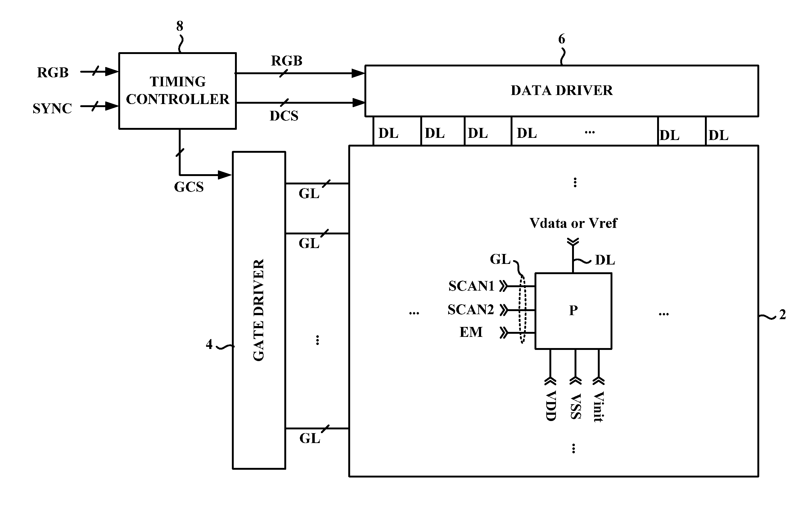
[0034]Reference will now be made in detail to the preferred embodiments of the present invention associated with an organic light emitting diode display device and a method for driving the same, examples of which are illustrated in the accompanying drawings.

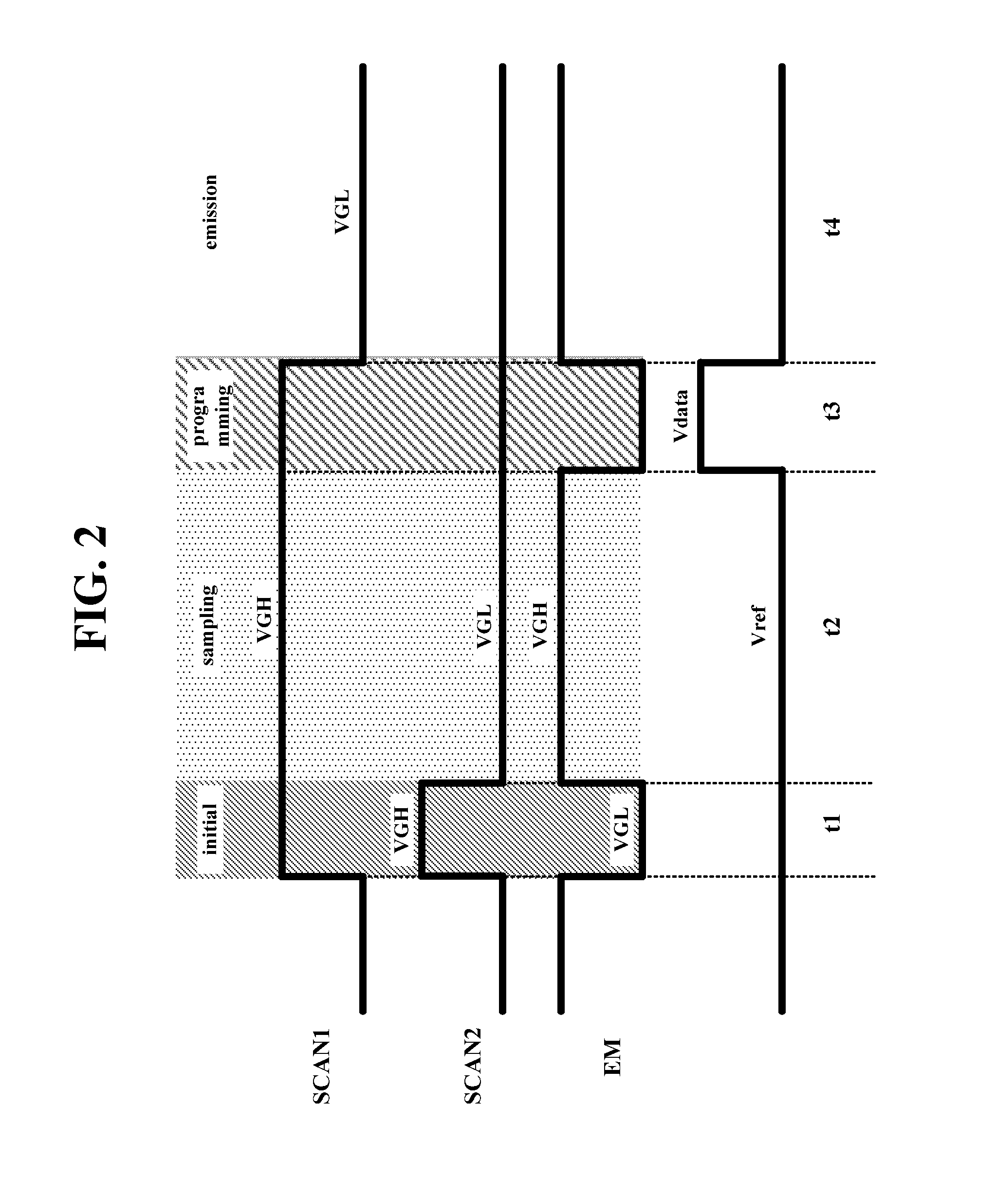
[0035]Thin film transistors (TFTs) employed in the present invention may be of a P type or an N type. The following description will be given in conjunction with the case in which TFTs are of an N type, for convenience of description. In this regard, gate high voltage VGH is a gate-on voltage to turn on a TFT, and gate low voltage VGL is a gate-off voltage to turn off a TFT. In explaining pulse type signals, gate high voltage (VGH) state is defined as a “high state”, and gate low voltage (VGL) state is defined as a “low state”.

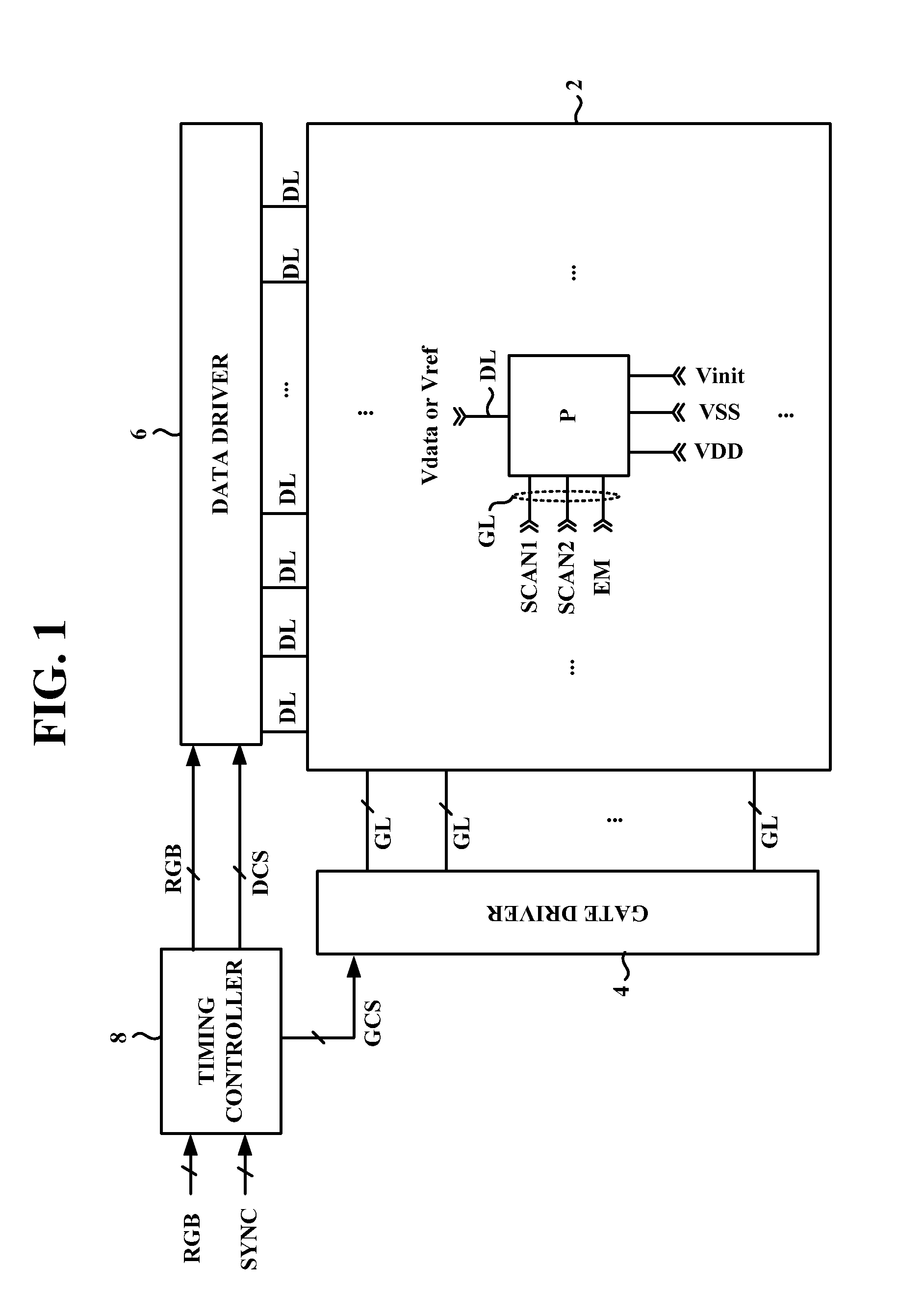
[0036]FIG. 1 is a block diagram illustrating a configuration of an organic light emitting diode (OLED) display device according to an exemplary embodiment of the present invention.

[0037]As illustrated in FI...


PUM


Abstract

Discussed are an organic light emitting diode (OLED) display device and a method for driving the same. The OLED display device includes pixels each including a light emitting element, and a pixel driving circuit. The pixel driving circuit includes a driving switching element connected in series between high and low-level voltage supply lines, together with the light emitting element, a first switching element for connecting a data line and a first node connected to a gate of the driving switching element in response to a first scan signal, a second switching element for connecting an initialization voltage supply line and a second node connected to a source of the driving switching element in response to a second scan signal, and a third switching element for connecting the high-level voltage supply line and a drain of the driving switching element in response to an emission signal.

Description

[0001]This application claims the benefit of the Korean Patent Application No. 10-2012-0157007, filed on Dec. 28,2012, which is hereby incorporated by reference as if fully set forth herein.BACKGROUND OF THE INVENTION[0002]1. Field of the Invention[0003]The present invention relates to an organic light emitting diode (OLED) display device and a method for driving the same.[0004]2. Discussion of the Related Art[0005]Each of Pixels constituting an OLED display device includes an OLED constituted by an anode, a cathode, and an organic light emitting layer interposed between the anode and the cathode, and a pixel circuit for independently driving the OLED. The pixel circuit mainly includes a switching thin film transistor (TFT), a capacitor, and a driving TFT. The switching TFT charges a data voltage in the capacitor in response to a scan pulse. The driving TFT controls an amount of current supplied to the OLED in accordance with the data voltage charged in the capacitor, to adjust an e...

Claims


Application Information

Patent Timeline
IPC IPC(8): G09G3/32
CPCG09G3/3241G09G3/3225G09G3/3233G09G2300/0814G09G2300/0819G09G2300/0852G09G2300/0861G09G2320/045G09G2300/0809G09G3/30
Inventor YOON, SANG-HUNLEE, JUNG-MIN
Owner LG DISPLAY CO LTD
Why Eureka
Try Eureka