High temperature sensor wafer for in-situ measurements in active plasma

a high temperature sensor and active plasma technology, applied in the direction of measurement devices, heat measurement, instruments, etc., can solve the problems of ensuing integrated circuits or devices to perform at a substandard level, failure to completely, and numerous processing steps

Active Publication Date: 2014-07-10
KLA TENCOR TECH CORP
View PDF1 Cites 15 Cited by
  • Summary
  • Abstract
  • Description
  • Claims
  • Application Information

AI Technical Summary

Benefits of technology

[0008]According to aspects of the present disclosure, a component module in a process condition measuring device comprises a support configured to support a component; one or more legs configured to suspend the support in a spaced-apart relationship with respect to a substrate; and an electrically conductive or low-resistivity semiconductor enclosure configured to enclose the component, the support and the legs between the substrate and the enclosure.
[0009]According to additional aspects of the present disclosure, a process condition measuring device comprises a substrate; and one or more component modules mounted on the substrate. The one or more component modules include a support for supporting a co

Problems solved by technology

Semiconductor fabrication generally involves numerous sophisticated and complex processing steps.
Any deviation from optimal processing conditions may cause the ensuing integrated circuit or device to perform at a substandard level or, worse yet, fail completely.
In general, the back AR coating (BARC) process operates at 250° C.; a PVD process may operate at about 300° C. and a CVD process may operate at a temperature of about 500° C. Unfortunately, batteries and microprocessors suitable

Method used


Image

  • High temperature sensor wafer for in-situ measurements in active plasma
  • High temperature sensor wafer for in-situ measurements in active plasma
  • High temperature sensor wafer for in-situ measurements in active plasma

Examples


Embodiment Construction

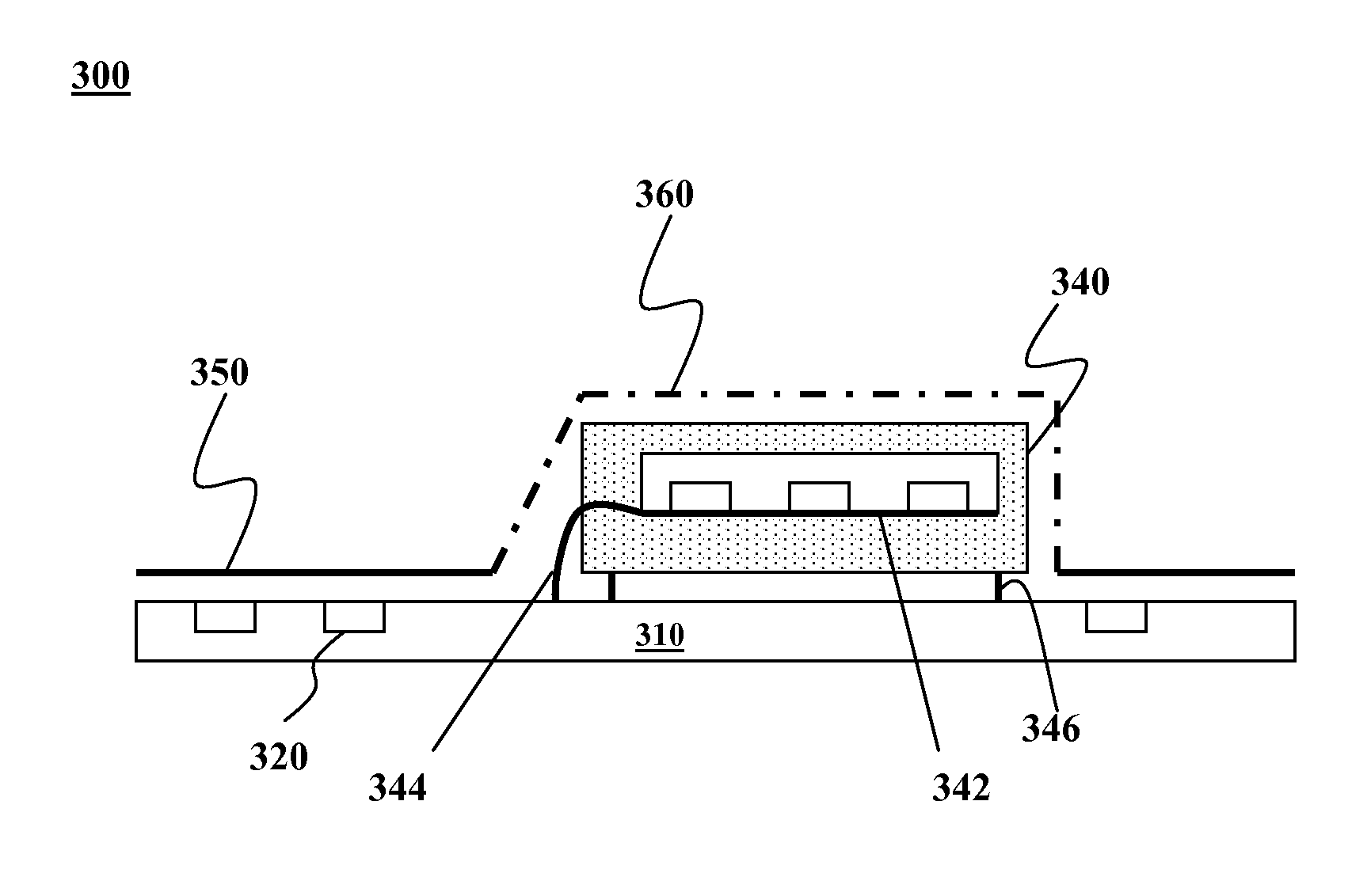
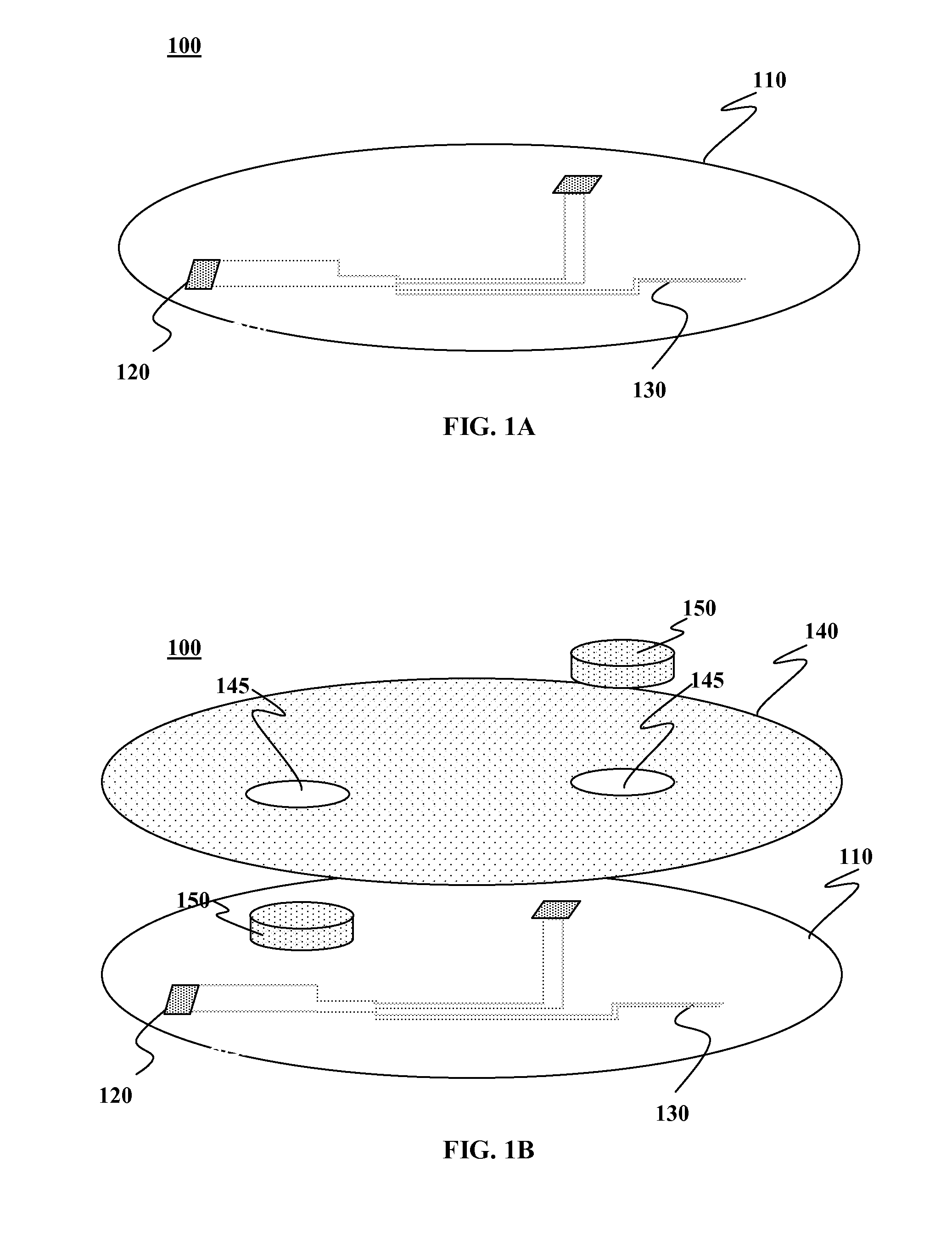
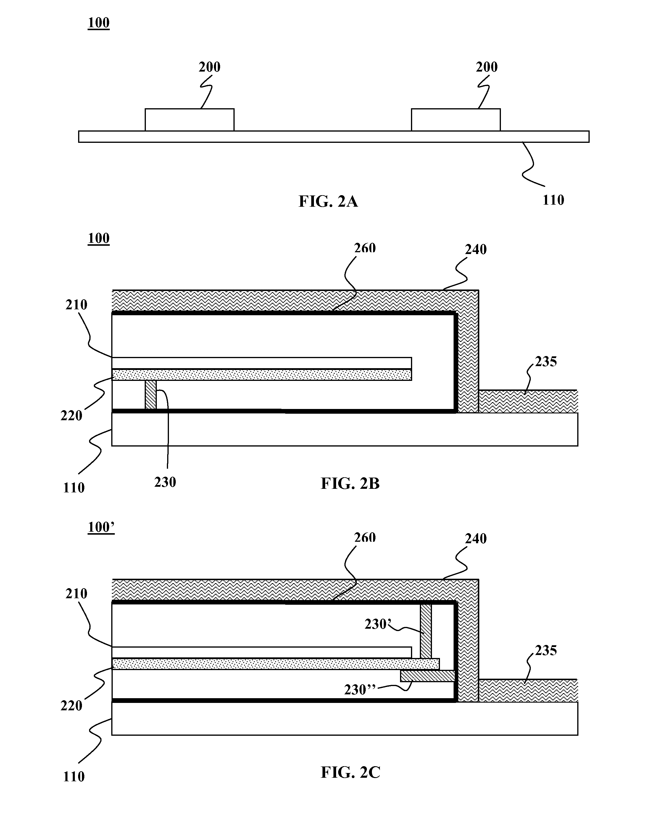
[0018]Although the following detailed description contains many specific details for the purposes of illustration, anyone of ordinary skill in the art will appreciate that many variations and alterations to the following details are within the scope of the invention. Accordingly, the exemplary embodiments of the invention described below are set forth without any loss of generality to, and without imposing limitations upon, the claimed invention. Additionally, because components of embodiments of the present invention can be positioned in a number of different orientations, the directional terminology is used for purposes of illustration and is in no way limiting. It is to be understood that other embodiments may be utilized and structural or logical changes may be made without departing from the scope of the present invention.

[0019]In this document, the terms “a” and “an” are used, as is common in patent documents, to include one or more than one. In this document, the term “or” is...


PUM


Abstract

Aspects of the present disclosure disclose a component module in a process condition measuring device comprises a support for supporting a component, one or more legs configured to suspend the support in a spaced-apart relationship with respect to a substrate. An electrically conductive or low-resistivity semiconductor enclosure is configured to enclose the component, the support and the legs between the substrate and the enclosure. It is emphasized that this abstract is provided to comply with the rules requiring an abstract that will allow a searcher or other reader to quickly ascertain the subject matter of the technical disclosure. It is submitted with the understanding that it will not be used to interpret or limit the scope or meaning of the claims.

Description

CLAIM PRIORITY[0001]This application claims the priority benefit of commonly owned, co-pending U.S. Provisional Patent Application No. 61 / 749,872, to Mei Sun, filed Jan. 7, 2013, and entitled “HIGH TEMPERATURE SENSOR WAFER FOR IN-SITU MEASUREMENTS IN ACTIVE PLASMA” the entire disclosures of which are incorporated herein by reference.FIELD OF THE INVENTION[0002]Embodiments of the present invention relate to high temperature process condition measuring devices, and more particularly to an apparatus and a method that keeps the components of the measuring device at an appropriate operating temperature and isolated from the plasma while the device is exposed in a high temperature environment and / or an operational plasma processing environment over an extend period of time.BACKGROUND OF THE INVENTION[0003]Semiconductor fabrication generally involves numerous sophisticated and complex processing steps. Monitoring and evaluation of each process step is crucial to ensure the manufacturing ac...

Claims


Application Information

Patent Timeline
IPC IPC(8): G01K1/14
CPCG01K1/14G01K1/12G01K2215/00
Inventor SUN, MEIJENSEN, EARLQULI, FARHATSHARRATT, STEPHEN
Owner KLA TENCOR TECH CORP
Why Eureka
Try Eureka