

Deposition mask, producing method therefor and forming method for thin film pattern
- Summary
- Abstract
- Description
- Claims
- Application Information
AI Technical Summary
Benefits of technology
Problems solved by technology
Method used
Image

Examples
Example
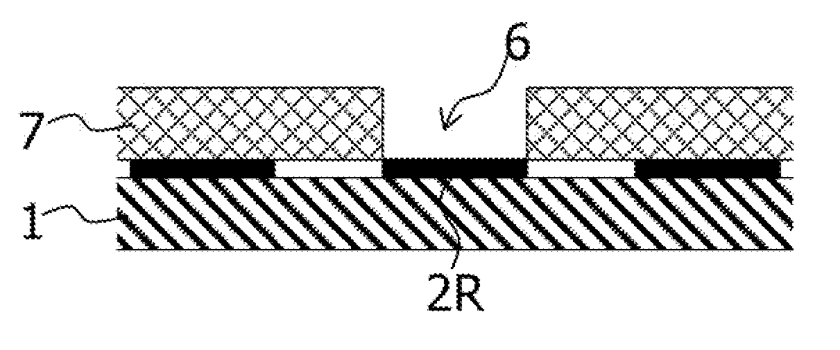
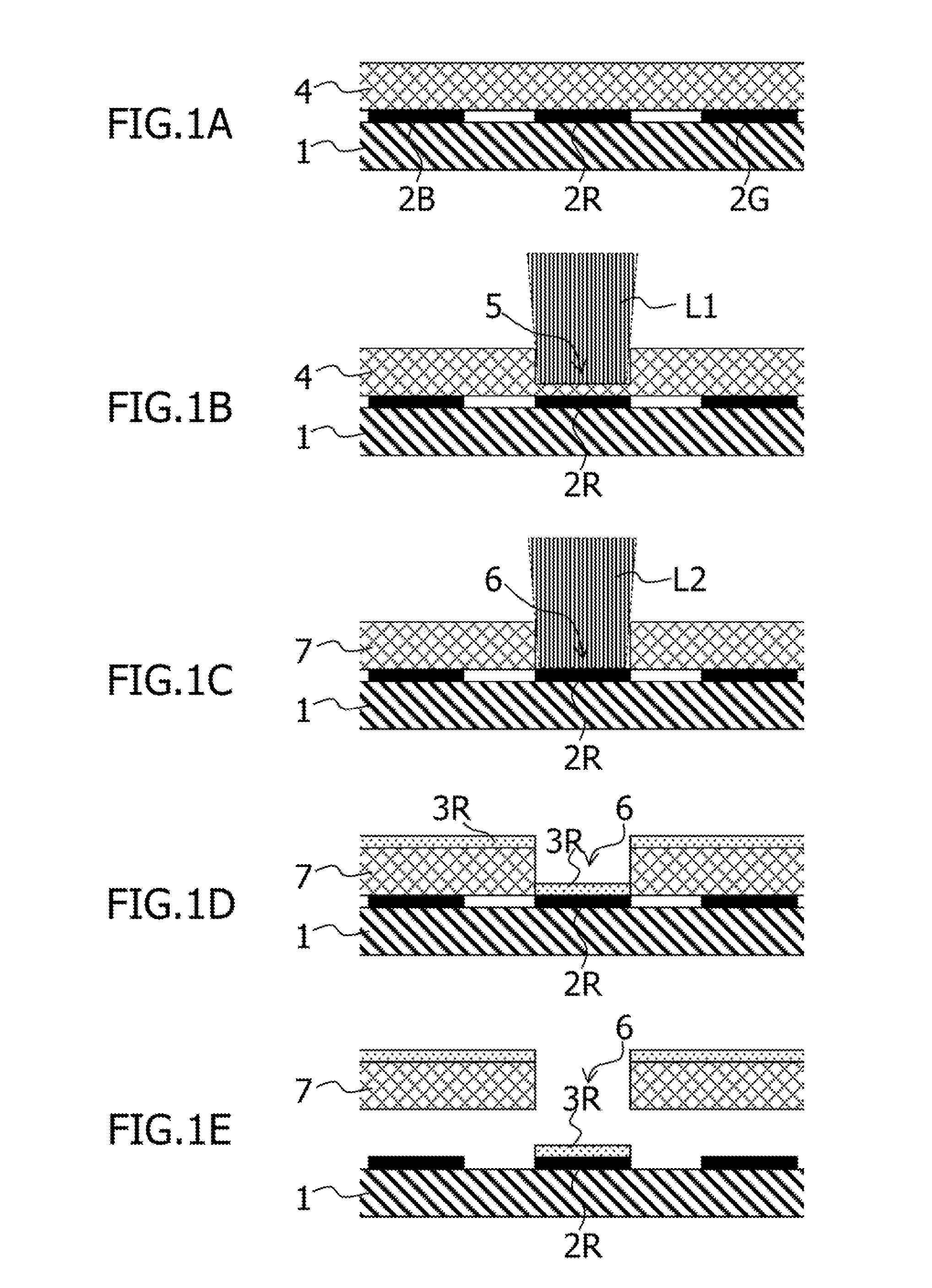
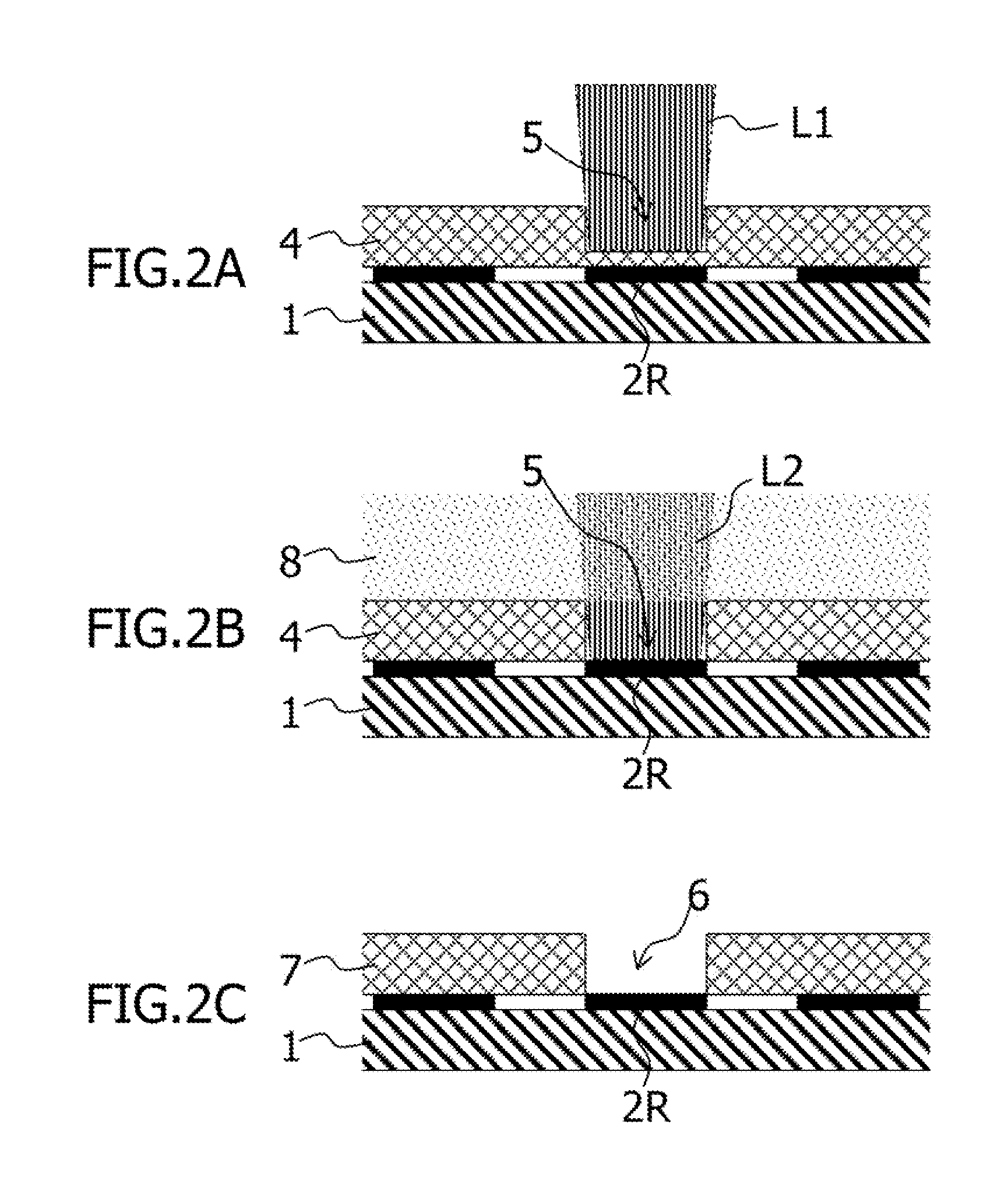
[0079]The first embodiment of the method for forming a thin film pattern includes a first step of placing a film 4 that is made of a resin transmitting visible light on a TFT substrate (it may be simply referred to as “substrate”) 1; a second step 2 of irradiating an anode electrode 2R portion for R on a TFT substrate 1 with laser light L1 having a predetermined energy density to dig the portion of the film 4 at a predetermined speed to a predetermined depth to form a hole 5, and processing a bottom portion of the hole 5 at a speed slower than the above speed to make the hole 5 penetrate through the film to thereby form a first embodiment of the deposition mask 7 of the present invention having an opening pattern 6 having the same shape and dimension as those of an R organic layer 3R; a third step of forming the R organic EL layer 3R on the anode electrode 2R for R by deposition through the opening pattern 6 of the deposition mask 7; and a step 4 of detaching the deposition mask 7.
[...
Example
[0099]Next, a second embodiment of the method for forming a thin film pattern of the present invention will be explained. Here, in the same manner as the above, explanation will be made with respect to a method for producing an organic EL display device by the second embodiment of the method for forming a thin film pattern in which the thin film pattern is an organic EL layer. In this method for producing an organic EL display device, the organic EL display device is produced by forming organic EL layer having a corresponding color on anode electrodes formed on the TFT substrate 1, and the method includes a process for forming a red (R) organic EL layer, a process for forming a green (G) organic EL layer, a process for forming a blue (B) organic EL layer, and a process for forming cathode electrodes.
[0100]FIGS. 4A to 4G are cross-sectional views illustrating the process for forming an R organic EL layer. In this process for forming an R organic EL layer, an organic material is heate...
Example
[0143]FIGS. 12A to 12E are process views illustrating a third embodiment of the method for producing the deposition mask of the present invention. This method for producing a deposition mask includes a first step of forming the metal member 10; a second step of retaining the resin film 4 by bringing it into close contact with the metal member 10; a third step of bringing the film 4 into close contact with the substrate 38; a fourth step of forming a plurality of opening patterns 6 in the film 4; and a fifth step of detaching the metal member 10 and the film 4 together from the substrate 38. In this method, a deposition mask illustrated in FIGS. 13A and 13B or FIG. 14 is produced.
[0144]Here, the deposition mask includes the film 4 that is made of a resin such as polyimide or polyethylene terephthalate (PET) transmitting visible light and that has the opening pattern 6 penetrating through the film 4 and having the same shape and dimension as those of a thin film pattern so as to corre...
PUM
| Property | Measurement | Unit |
|---|---|---|
| Wavelength | aaaaa | aaaaa |
| Temperature | aaaaa | aaaaa |
| Thickness | aaaaa | aaaaa |
Abstract
Description
Claims
Application Information