Multi-layer micro-wire structure

a micro-wire and multi-layer technology, applied in the direction of light absorption dielectrics, semiconductor/solid-state device details, instruments, etc., can solve the problems of increasing material cost, relatively expensive depositing and patterning, and limited conductivity and transparency of metal oxides, so as to improve flexibility, contrast, or reflectivity, the effect of improving flexibility

Inactive Publication Date: 2014-08-28
EASTMAN KODAK CO
View PDF6 Cites 10 Cited by
  • Summary
  • Abstract
  • Description
  • Claims
  • Application Information

AI Technical Summary

Benefits of technology

[0014]The present invention provides an electrically conductive micro-wire structure having improved transparency, contrast, or reflectivity, improved flexibility, and resistance to scratches.

Problems solved by technology

Such materials are increasingly expensive and relatively costly to deposit and pattern.
Moreover, metal oxides have a limited conductivity and transparency, and tend to crack when formed on flexible substrates.

Method used


Image

  • Multi-layer micro-wire structure
  • Multi-layer micro-wire structure
  • Multi-layer micro-wire structure

Examples


Embodiment Construction

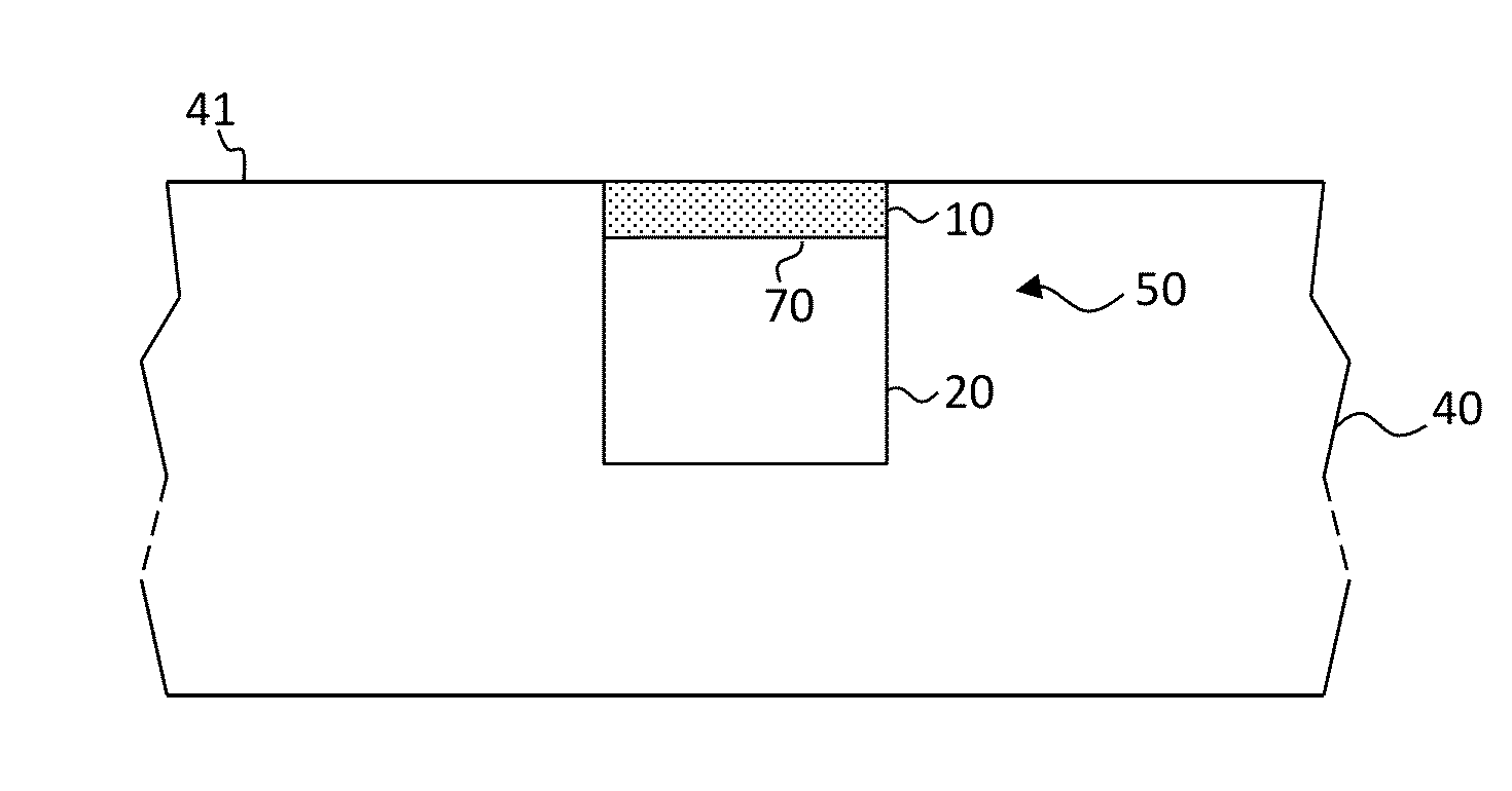
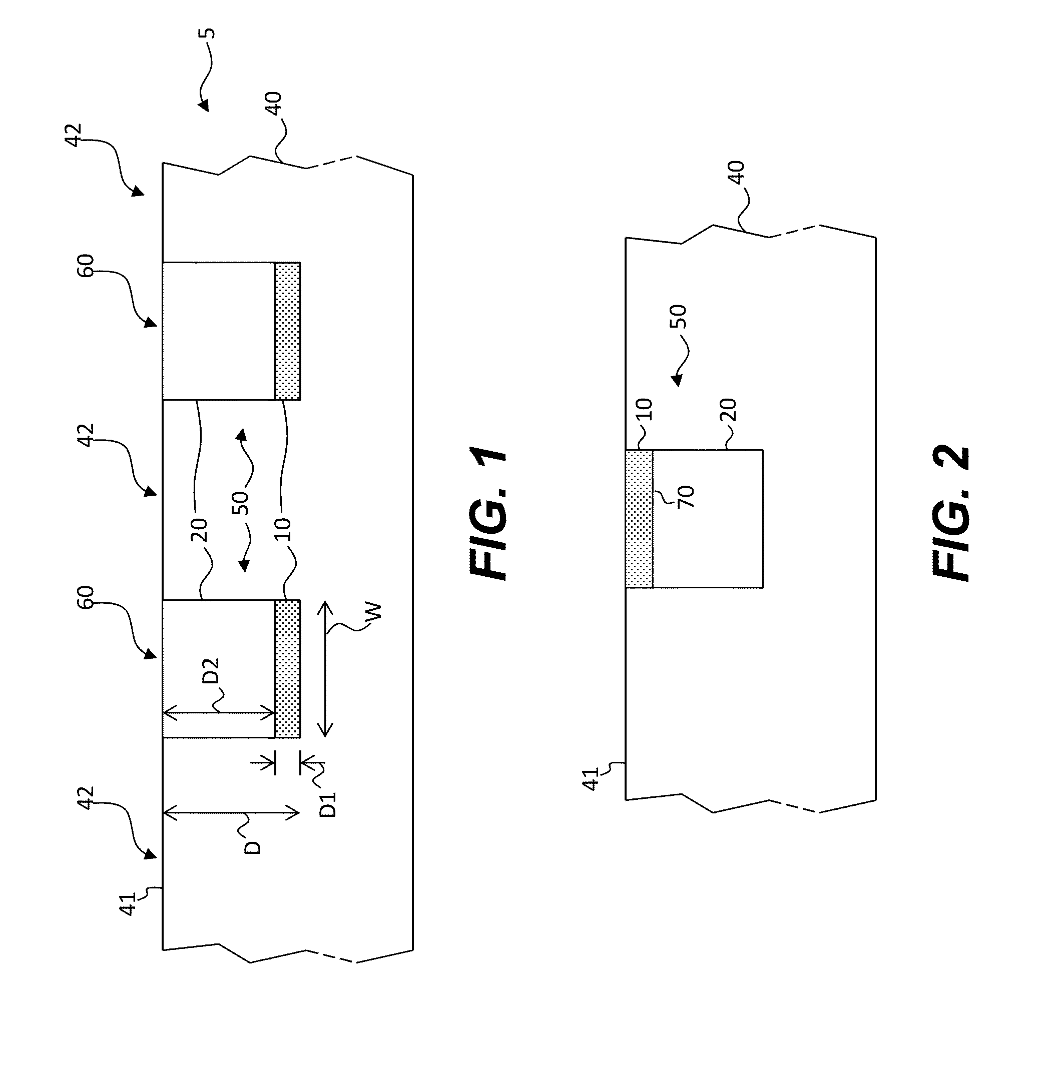
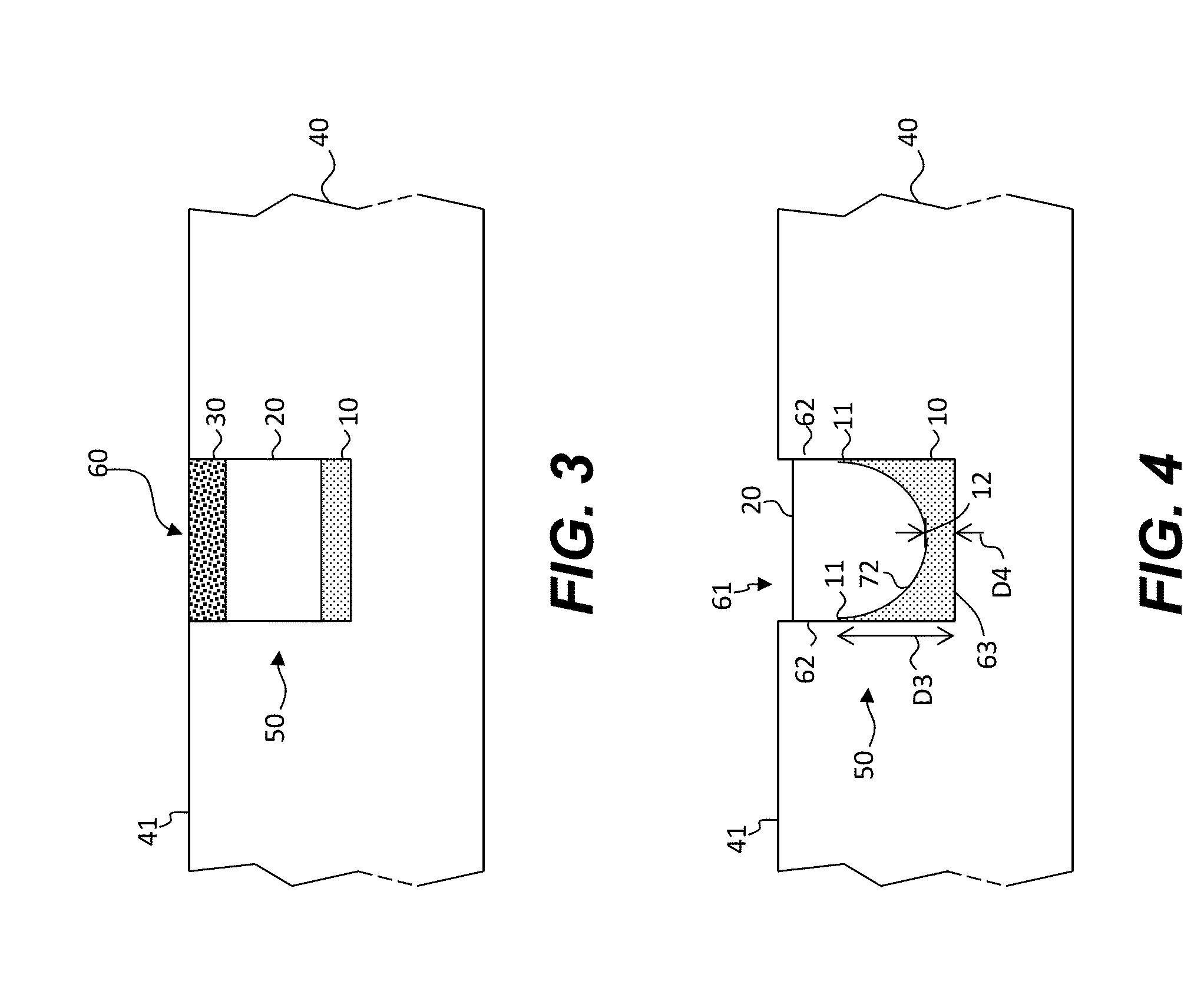
[0028]The present invention is directed toward multi-layer micro-wire structures formed in a substrate that are capable of conducting electrical currents. The electrically conductive micro-wire structures provide improved transparency, contrast, or reflectivity, improved flexibility, and resistance to scratches.

[0029]Referring to FIG. 1 in an embodiment of the present invention, a multi-layer micro-wire structure 5 includes a substrate 40 having a substrate surface 41. A plurality of micro-channels 60 are formed in substrate 40. Substrate-surface open areas 42 on substrate 40 separate micro-channels 60. Micro-channels 60 extend from substrate surface 41 into substrate 40. A first material composition is located in a first layer 10 in each micro-channel 60 and not on substrate surface 41 and not in substrate-surface open areas 42 between micro-channels 60. A second material composition different from the first material composition is located in a second layer 20 different from first ...


PUM

PropertyMeasurementUnit
widthaaaaaaaaaa
widthaaaaaaaaaa
widthaaaaaaaaaa

Abstract

A multi-layer micro-wire structure includes a substrate having a surface. A plurality of micro-channels is formed in the substrate. A first material composition is located in a first layer only in each micro-channel and not on the substrate surface. A second material composition different from the first material composition is located in a second layer different from the first layer only in each micro-channel and not on the substrate surface. The first material composition in the first layer and the second material composition in the second layer form an electrically conductive multi-layer micro-wire in each micro-channel.

Description

CROSS REFERENCE TO RELATED APPLICATION[0001]Reference is made to commonly-assigned U.S. patent application Ser. No. ______(Docket K001393) filed concurrently herewith, entitled “Making Multi-Layer Micro-Wire Structure” by Yau et al, the disclosure of which is incorporated herein.FIELD OF THE INVENTION[0002]The present invention relates to micro-wire electrical conductors.BACKGROUND OF THE INVENTION[0003]Transparent conductors are widely used in the flat-panel display industry to form electrodes for electrically switching the light-emitting or light-transmitting properties of a display pixel, for example in liquid crystal or organic light-emitting diode displays. Transparent conductive electrodes are also used in touch screens in conjunction with displays. In such applications, the transparency and conductivity of the transparent electrodes are important attributes. In general, it is desired that transparent conductors have a high transparency (for example, greater than 90% in the vi...

Claims


Application Information

Patent Timeline
Patent Type & Authority Applications(United States)
IPC IPC(8): H01L33/42
CPCG02F1/00G02F1/13439G06F2203/04103H05K3/0014H05K2201/0108H05K2201/0112H05K2201/0257H05K2201/0338H05K2201/2054H05K2203/1131H05K2203/1476H05K3/1258H05K2201/0269H05K2201/0272H05K2201/0376H05K2203/0108G06F3/0443G01N27/07G01N27/126
Inventor YAU, HWEI-LINGTRAUERNICHT, DAVID PAULLEBENS, JOHN ANDREWWANG, YONGCAICOK, RONALD STEVEN
Owner EASTMAN KODAK CO
Why Eureka
Try Eureka