Memory Device And Electronic Device

a technology of electronic devices and memory devices, applied in the field of memory devices, can solve the problem of taking a long time for data writing, and achieve the effect of reducing the circuit area

Active Publication Date: 2014-09-25
SEMICON ENERGY LAB CO LTD
View PDF3 Cites 0 Cited by
  • Summary
  • Abstract
  • Description
  • Claims
  • Application Information

AI Technical Summary

Benefits of technology

This patent describes an invention that reduces voltage changes in a data line caused by leakage current in an output transistor. This is accomplished by using a transistor as the output transistor that has two gates, one of which is connected to the source and drain of the output transistor and the other of which is connected to the source and drain of a selection transistor. This configuration helps to minimize the impact of leakage current on the data line. Additionally, placing the output transistor over the selection transistor reduces the circuit area.

Problems solved by technology

However, in the conventional memory device that is described above, a selection operation is performed for the memory cells in each row and cannot be performed for the individual memory cells.
Thus, it takes a long time for data writing.

Method used


Image

  • Memory Device And Electronic Device
  • Memory Device And Electronic Device
  • Memory Device And Electronic Device

Examples


embodiment 1

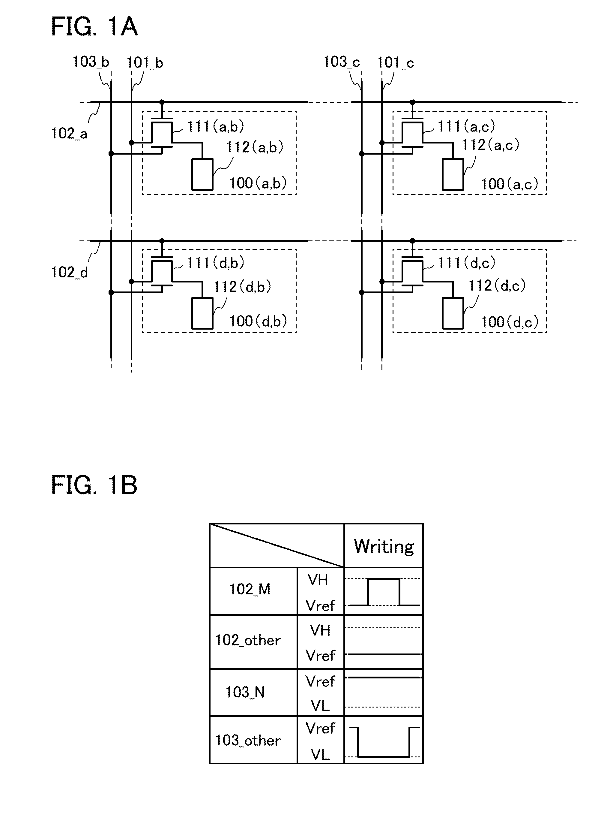
[0039]In this embodiment, an example of a memory device in which a selection operation can be performed for individual memory cells is described.

[0040]An example of the memory device in this embodiment includes three or more memory cells which are arranged in the row and column directions. The memory cells are provided in a memory cell array, for example.

[0041]An example of the memory device in this embodiment is described with reference to FIGS. 1A and 1B.

[0042]First, an example of a structure of the memory device in this embodiment is described with reference to FIG. 1A.

[0043]The memory device illustrated in FIG. 1A includes a memory cell 100 (a,b) (a and b are natural numbers), a memory cell 100 (a,c) (c is a natural number larger than a), a memory cell 100 (d,b) (d is a natural number larger than b), and a memory cell 100 (d,c). Note that the memory cell 100 (d,c) is not necessarily provided. Further, a memory cell other than the memory cell 100 (a,b), the memory cell 100 (a,c),...

embodiment 2

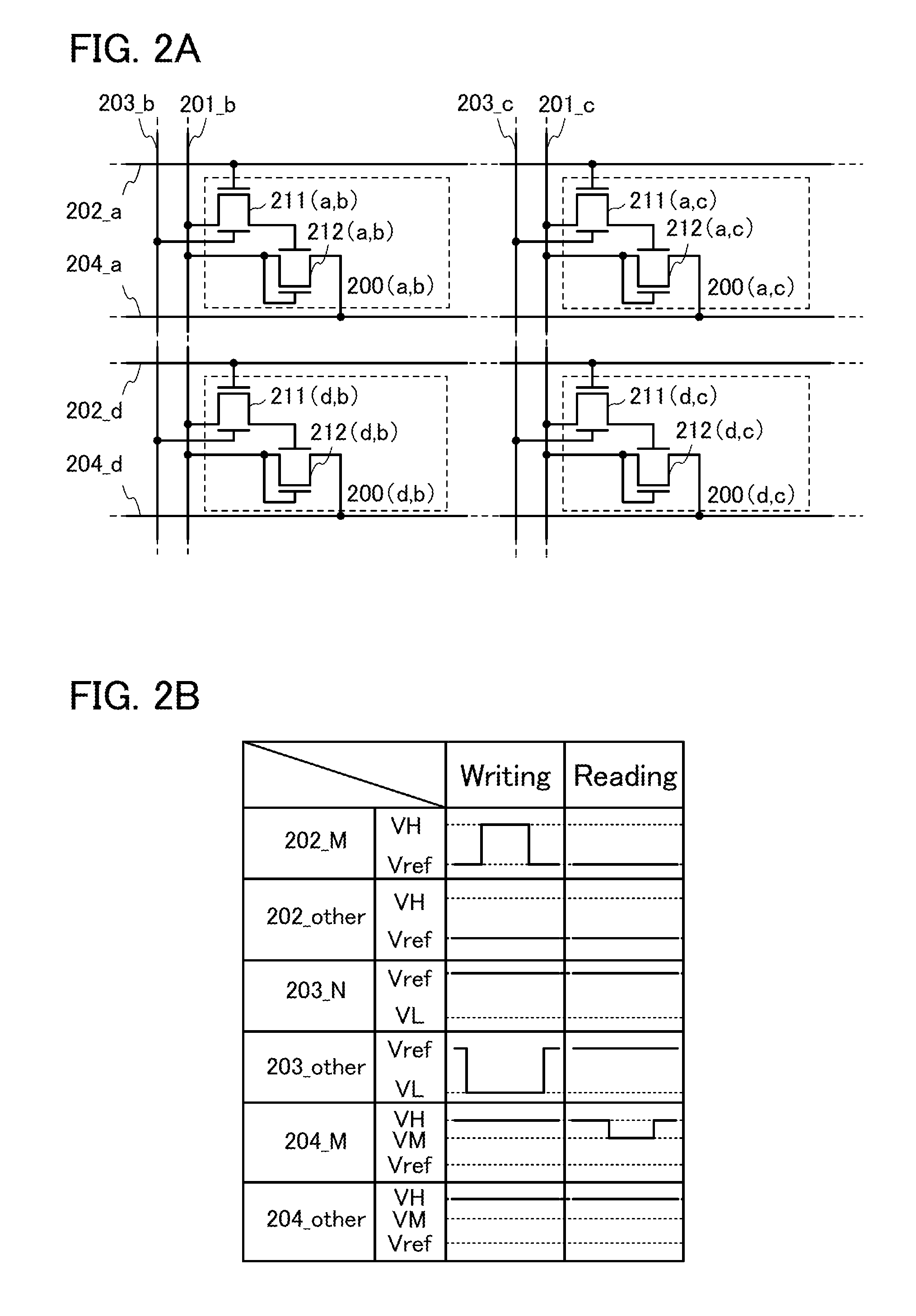
[0077]In this embodiment, an example of the memory device in Embodiment 1 is described.

[0078]An example of the memory device in this embodiment is described with reference to FIGS. 2A and 2B.

[0079]First, an example of a structure of the memory device in this embodiment is described with reference to FIG. 2A.

[0080]The memory device illustrated in FIG. 2A includes a memory cell 200 (a,b), a memory cell 200 (a,c), a memory cell 200 (d,b), and a memory cell 200 (d,c). Note that the memory cell 200 (d,c) is not necessarily provided. Further, a memory cell other than the memory cell 200 (a,b), the memory cell 200 (a,c), the memory cell 200 (d,b), and the memory cell 200 (d,c) may be provided. Further, a memory cell may be provided at any one or more of the following positions: between the memory cell 200 (a,b) and the memory cell 200 (a,c), between the memory cell 200 (a,b) and the memory cell 200 (d,b), between the memory cell 200 (d,b) and the memory cell 200 (d,c), and between the memo...

embodiment 3

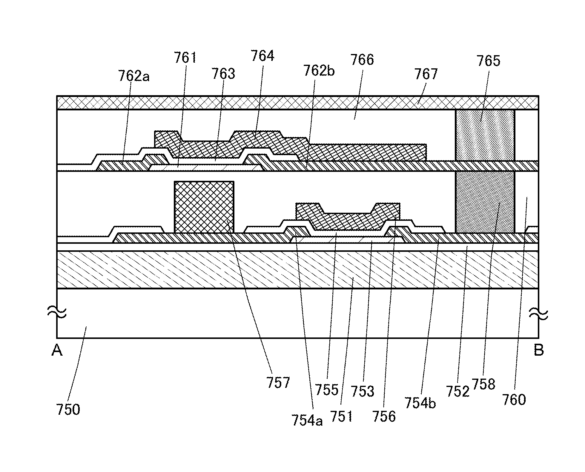
[0128]In this embodiment, an example of a structure of a memory cell in the memory device in Embodiment 2 is described with reference to FIGS. 4A and 4B. FIGS. 4A and 4B illustrate an example of a structure of the memory cell in this embodiment. An example of a structure of the memory cell illustrated in FIGS. 2A and 2B is described here as an example. Note that the components illustrated in FIGS. 4A and 4B include those having sizes different from the actual sizes.

[0129]The memory cell illustrated in FIGS. 4A and 4B includes a conductive layer 751, an insulating layer 752, a semiconductor layer 753, a conductive layer 754a, a conductive layer 754b, an insulating layer 755, a conductive layer 756, a conductive layer 757, a conductive layer 758, an insulating layer 760, a semiconductor layer 761, a conductive layer 762a, a conductive layer 762b, an insulating layer 763, a conductive layer 764, a conductive layer 765, an insulating layer 766, and a conductive layer 767.

[0130]The condu...


PUM


Abstract

A selection operation is performed for individual memory cells. A device includes a first memory cell and a second memory cell provided in the same row as the first memory cell, each of which includes a field-effect transistor having a first gate and a second gate. The field-effect transistor controls at least data writing and data holding in the memory cell by being turned on or off. The device further includes a row selection line electrically connected to the first gates of the field-effect transistors included in the first memory cell and the second memory cell, a first column selection line electrically connected to the second gate of the field-effect transistor included in the first memory cell, and a second column selection line electrically connected to the second gate of the field-effect transistor included in the second memory cell.

Description

CROSS-REFERENCE TO RELATED APPLICATIONS[0001]This application is a continuation of U.S. application Ser. No. 13 / 418,546, filed Mar. 13, 2012, now allowed, which claims the benefit of a foreign priority application filed in Japan as Serial No. 2011-060175 on Mar. 18, 2011, both of which are incorporated by reference.BACKGROUND OF THE INVENTION[0002]1. Field of the Invention[0003]One embodiment of the present invention relates to a memory device.[0004]2. Description of the Related Art[0005]In recent years, a variety of memory devices capable of rewriting data have been developed.[0006]As an example of such a memory device, a memory device in which a selection transistor is provided in each memory cell can be given (for example, see Patent Document 1).[0007]In the memory device in which the selection transistor is provided in the memory cell, a selection operation for the memory cell is performed by turning on the selection transistor, and an operation such as data writing is performed...

Claims


Application Information

Patent Timeline
Patent Type & Authority Applications(United States)
IPC IPC(8): H01L27/105
CPCH01L27/105G11C11/404G11C11/405H01L27/0688H01L27/1225H10B41/70G11C7/10G11C11/34H01L27/10H10B99/00G11C8/10H01L23/528H01L27/0629H01L29/7869
Inventor MATSUBAYASHI, DAISUKE
Owner SEMICON ENERGY LAB CO LTD
Why Eureka
Try Eureka