Method of forming a strained silicon layer

a technology of strained silicon and layer, applied in the field of forming a strained silicon layer, can solve the problem of a relatively high density of defects in the relaxed sige layer

Active Publication Date: 2014-09-25
STMICROELECTRONICS (CROLLES 2) SAS +1
View PDF6 Cites 14 Cited by
  • Summary
  • Abstract
  • Description
  • Claims
  • Application Information

AI Technical Summary

Benefits of technology

[0009]It is an aim of embodiments of the present disclosure to at least partially address one or more problems in the prior art.

Problems solved by technology

A problem with such existing techniques is that there tends to be a relatively high density of defects in the relaxed SiGe layer, which are then transferred to the epitaxial silicon layer.

Method used


Image

  • Method of forming a strained silicon layer
  • Method of forming a strained silicon layer
  • Method of forming a strained silicon layer

Examples


Embodiment Construction

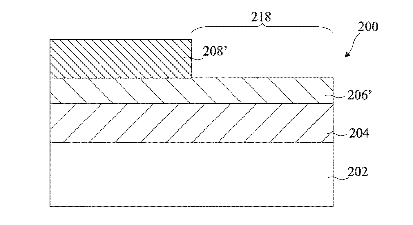
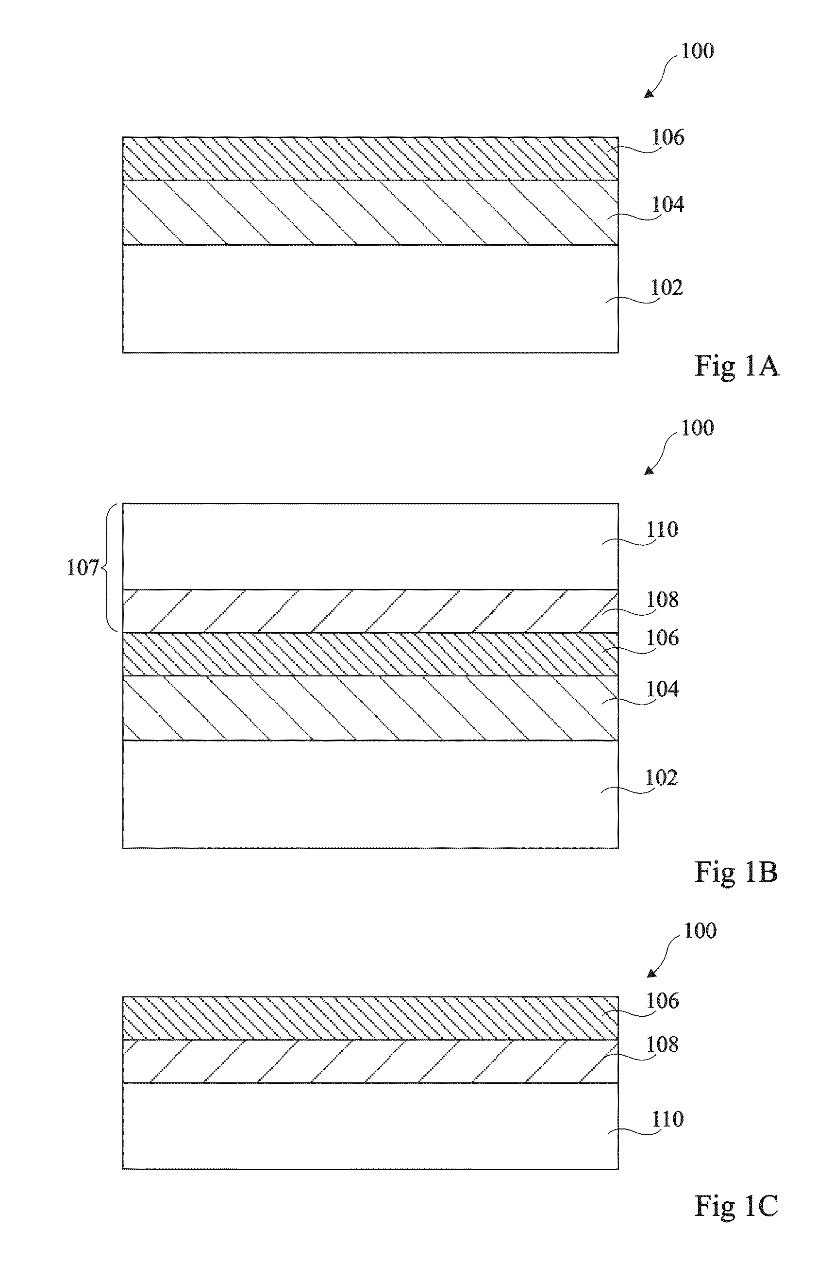
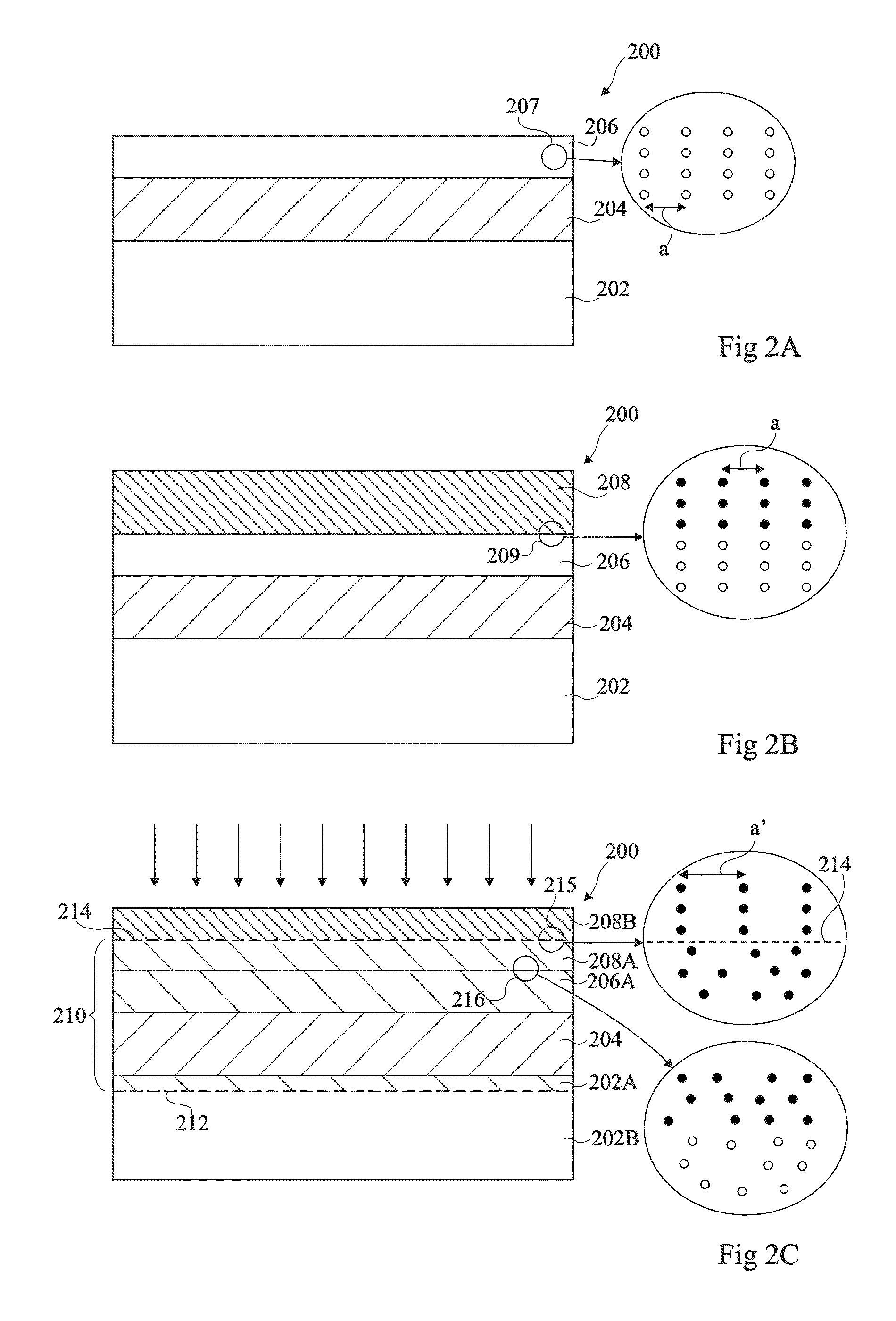
[0030]FIGS. 1A to 1C are cross-section views of a structure during successive steps in a method for forming a strained silicon layer.

[0031]FIG. 1A illustrates a structure 100 comprising a silicon substrate 102. A relaxed silicon germanium (SiGe) layer 104 has been formed by epitaxial growth over the silicon substrate 102. SiGe layer 104 for example comprises lower concentrations of germanium near the interface with the silicon substrate 102, and higher concentrations of germanium towards its upper surface. A silicon layer 106 has been formed by epitaxial growth over the SiGe layer 104, resulting in a strained silicon layer as the silicon atoms are stretched beyond their normal inter-atomic distance by the presence of the underlying SiGe layer 104.

[0032]FIG. 1B illustrates the silicon structure 100 after a subsequent step in which an oxidized silicon support substrate 107, comprising an oxide layer 108 and a silicon substrate 110, is bonded to the strained silicon layer 106.

[0033]FIG...


PUM

PropertyMeasurementUnit
thicknessaaaaaaaaaa
thicknessaaaaaaaaaa
thicknessaaaaaaaaaa

Abstract

The present disclosure concerns a method involving: forming a strained silicon germanium layer by epitaxial growth over a silicon layer disposed on a substrate; implanting atoms to amorphize the silicon layer and a lower portion of the silicon germanium layer, without amorphizing a surface portion of the silicon germanium layer; and annealing, to at least partially relax the silicon germanium layer and to re-crystallize the lower portion of the silicon germanium layer and the silicon layer, so that the silicon layer becomes a strained silicon layer.

Description

CROSS REFERENCE TO RELATED APPLICATIONS[0001]This application claims the priority benefit of French Patent Application No. 13 / 52497, filed on Mar. 20, 2013, entitled “Method of Forming a Strained Silicon Layer,” which is hereby incorporated by reference to the maximum extent allowable by law.BACKGROUND[0002]1. Technical Field[0003]The present disclosure relates to the field of silicon on insulator (SOI) structures, and in particular to a method of forming a strained silicon layer.[0004]2. Discussion of the Related Art[0005]In certain applications, such as for the formation of high performance transistors, it can be advantageous to use a strained silicon or silicon germanium layer. In particular, silicon layers that are in tension and / or compression demonstrate an increased speed of charge careers, thereby increasing performance of transistor devices formed within such layers.[0006]Existing techniques for forming a strained silicon layer generally involve forming the silicon layer by...

Claims


Application Information

Patent Timeline
Patent Type & Authority Applications(United States)
IPC IPC(8): H01L21/02
CPCH01L21/02694H01L21/02532H01L21/02502H01L21/02381H01L21/02488H01L21/0245H01L21/02002H01L21/823807H01L21/84H01L29/1054
Inventor HALIMAOUI, AOMARHARTMANN, JEAN-MICHEL
Owner STMICROELECTRONICS (CROLLES 2) SAS
Why Eureka
Try Eureka