Electrical Probe for Testing Electronic Device

a technology for electronic devices and probes, applied in electrical testing, measurement devices, instruments, etc., can solve the problems of electromagnetic interference to the associated electrical test, limited improvement of electrical connections, etc., and achieve the effect of increasing test accuracy

Inactive Publication Date: 2014-10-30
HSIAO TE HSING
View PDF9 Cites 2 Cited by
  • Summary
  • Abstract
  • Description
  • Claims
  • Application Information

AI Technical Summary

Benefits of technology

[0007]The primary object of the present invention is to provide an electrical probe, which comprises a cylindrical body which has a first end including a plurality of claws and a second end opposite to the first end for cooperating with an electrical test machine, wherein a concave contact surface conforming with the curvature of a solder ball of an electronic device under test is formed between the claws, whereby the first end of the cylindrical body can be brought into line contact with the solder ball at a predetermined length to ensure a proper electrical connection for increasing the test accuracy.

Problems solved by technology

However, in the test, since each tapered probe is in point contact with each solder ball, the tapered probes may not keep a proper election connection with the solder balls, and thus an inaccurate test may result.
Thus, the improvement of the electrical connection is limited.
Besides, when two objects are electrically connected through point contact, high voltage is prone to occur, and thus may cause an electromagnetic interference to the associated electrical test.

Method used


Image

  • Electrical Probe for Testing Electronic Device
  • Electrical Probe for Testing Electronic Device
  • Electrical Probe for Testing Electronic Device

Examples


Embodiment Construction

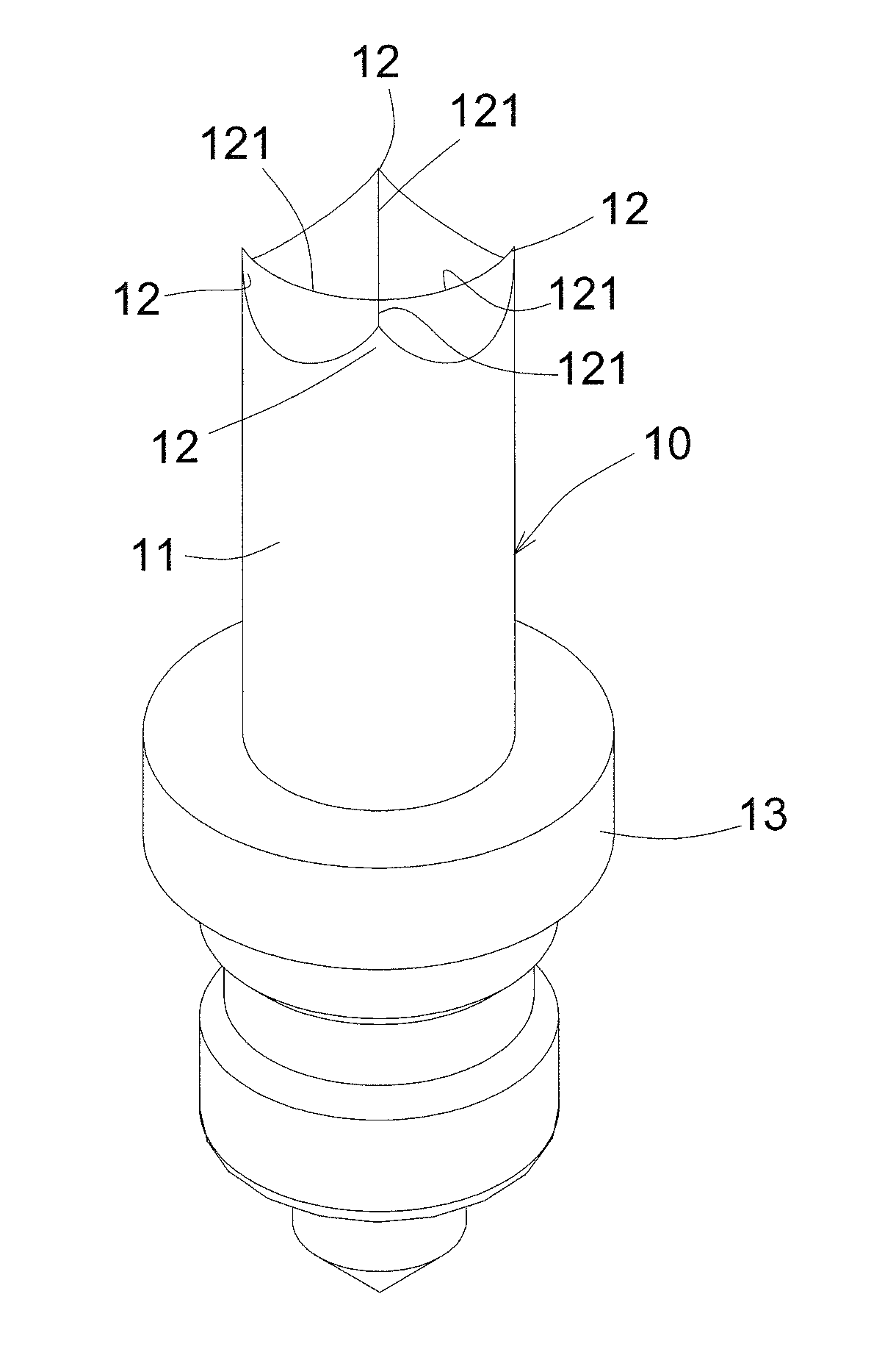
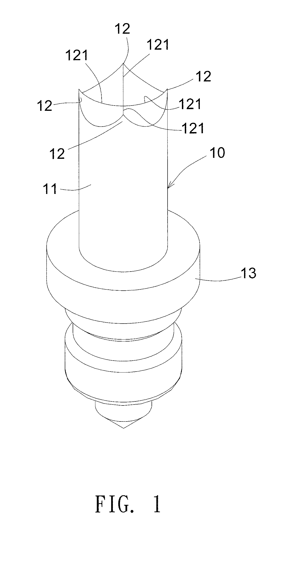
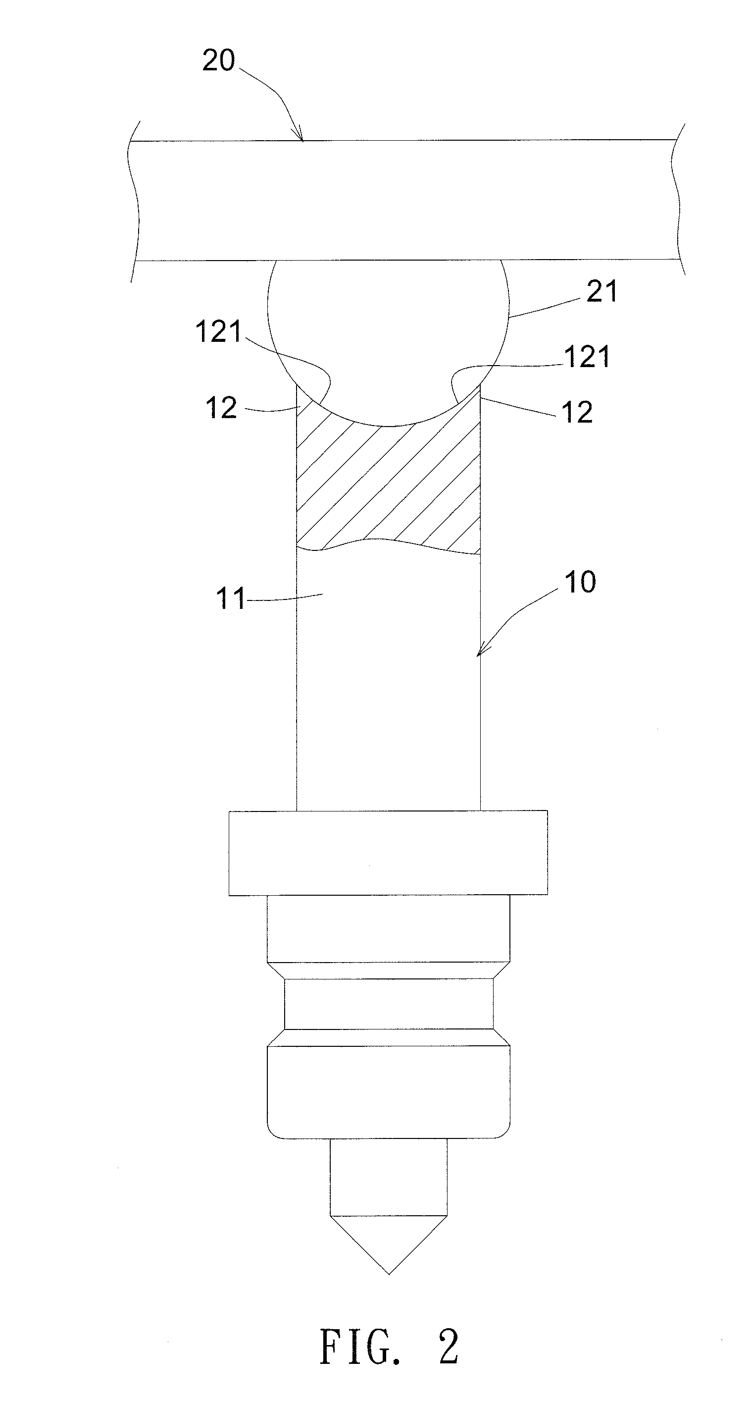
[0019]FIGS. 1 and 2 show embodiments, concerning an electrical probe (10), of the present invention, which generally comprise a cylindrical body (11) which has a first end including a plurality of claws (12) and a second end opposite to the first end for cooperating with a test machine. Furthermore, a concave contact surface (121), conforming with the curvature of a solder ball (21) of an electronic device under test (20), is defined between two adjacent claws (12). With these features, the contact area between the cylindrical body (11) and the solder ball (21) can be increased, and thus the test accuracy can be increased.

[0020]Although the accompanying drawings of the present invention show a specific number of claws (12), the electrical probe (10) can have other number of claws.

[0021]In manufacturing the electrical probe of the present invention, as shown in FIG. 3, a cylindrical cutter (C) having a length more than the diameter of the cylindrical body (11) and having a diameter s...


PUM


Abstract

An electrical probe comprises a cylindrical body which has a first end including a plurality of claws and a second end opposite to the first end for cooperating with an electrical test machine, wherein a concave contact surface conforming with the curvature of a solder ball of an electronic device under test is formed between the claws, whereby the first end of the cylindrical body can be brought into line contact with the solder ball at a predetermined length to ensure a proper electrical connection, so that the accuracy of an electrical test can be increased.

Description

TECHNICAL FIELD OF THE INVENTION[0001]The present invention relates to an electrical probe for testing an electronic device and, more particularly, to an electrical probe that includes a plurality of claws, between which a concave contact surface conforming with the curvature of the solder ball of the electronic device is formed, whereby the contact area between the electrical probe and the solder ball can be increased.DESCRIPTION OF THE PRIOR ART[0002]Microprocessors, which are a typical example of an integrated circuit, are usually fabricated in BGA (Ball Grid Array) package, which connects to a PCB (printed circuit board) via solder balls. For ensuring an electronic package to be correctly fabricated, electrical tests are required.[0003]Conventionally, for conducting an electrical test for an electronic device, tapered probes can be employed to touch the solder balls of the electronic device. However, in the test, since each tapered probe is in point contact with each solder ball...

Claims


Application Information

Patent Timeline
Patent Type & Authority Applications(United States)
IPC IPC(8): G01R1/067
CPCG01R1/067G01R1/06738G01R1/06722
Inventor HSIAO, TE-HSING
Owner HSIAO TE HSING
Why Eureka
Try Eureka