High performance printed circuit board

high-performance technology, applied in the direction of printed element electric connection formation, high-frequency circuit adaptation, instruments, etc., can solve the problems of limiting the area in which traces can be run, remaining plating can interfere with high-frequency operation, and can be particularly difficult to design a printed circuit board for the attachment of an electrical connector

Inactive Publication Date: 2014-11-06
AMPHENOL CORP
View PDF44 Cites 26 Cited by
  • Summary
  • Abstract
  • Description
  • Claims
  • Application Information

AI Technical Summary

Benefits of technology

This patent describes how to improve the design of high-frequency printed circuits by adding special areas called "breakout regions." These breaks help reduce problems with signals passing through different parts of the circuit. By adjusting certain factors about these breaks, they can minimize the impact on signal quality caused by changes in resistance levels. Overall, this helps make better designed printed circuits for use at higher frequencies.

Problems solved by technology

The technical problem addressed in this patent relates to improving the performance of printed circuit boards used in high-frequency applications. Specifically, there are issues related to connecting components like electrical connectors and reducing interference between neighboring traces while maintaining good contact. Various solutions include adding ground planes, optimizing impedance matching, back drilling to remove excess plating, and utilizing differential paired signals.

Method used


Image

  • High performance printed circuit board
  • High performance printed circuit board
  • High performance printed circuit board

Examples


Embodiment Construction

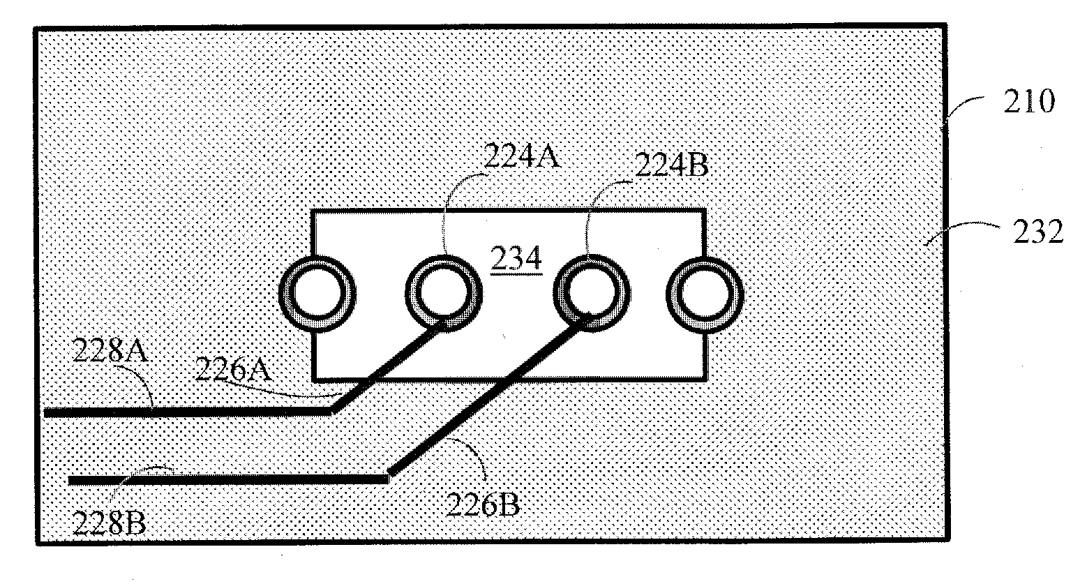
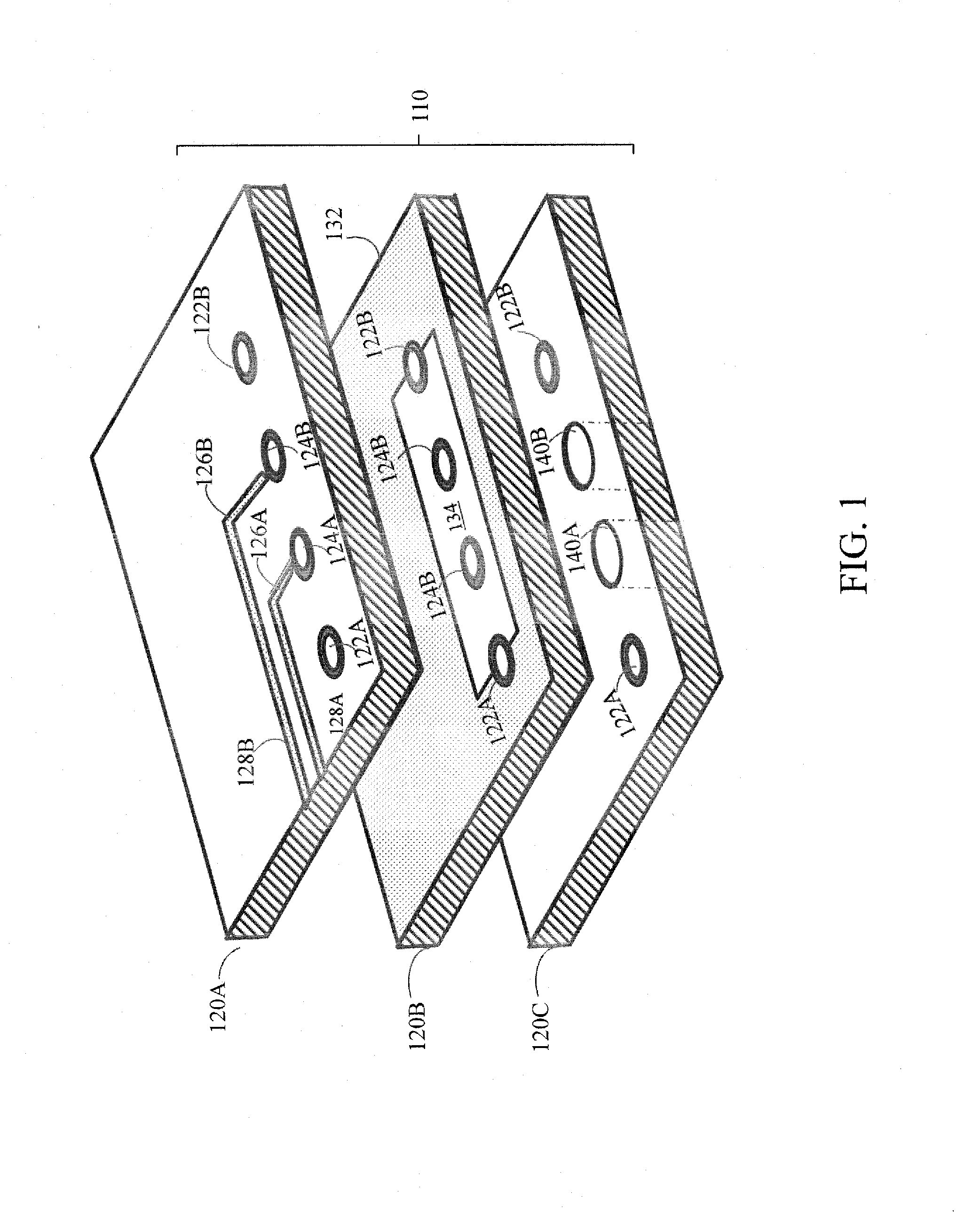
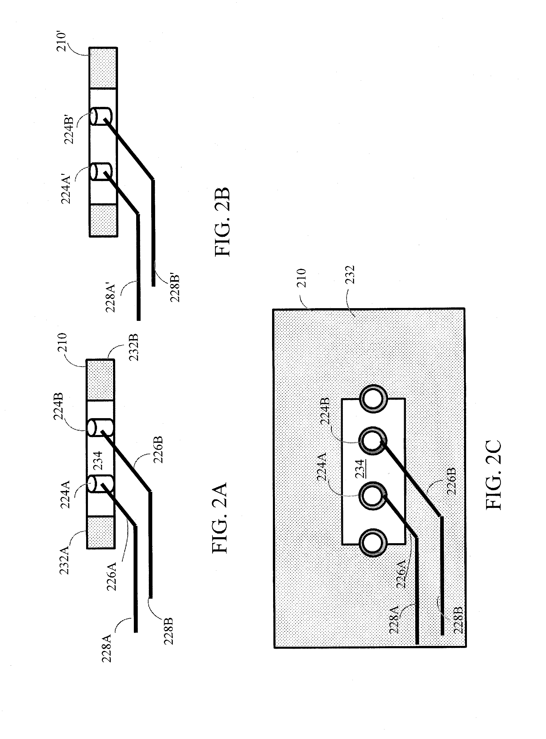
[0039]The inventor has recognized and appreciated that improved high frequency performance of a printed circuit board may be achieved by controlling the impedance of breakout regions within a footprint for a connector or other component to be mounted to a printed circuit board. The impedance may be controlled to reduce the number of impedance transitions in the signal paths that carry high speed signals through the printed circuit board. The inventor has recognized and appreciated that, though the breakout region may be a relatively small portion of the overall signal path through a via and along traces of the printed circuit board, impedance characteristics in the breakout region can have a significant impact on the integrity of signals propagating along that path.

[0040]Further, the inventor has recognized and appreciated that, at high frequencies, such as those associated with signals with data rates above 3 Gigabits per second (Gbps), patterns of changes in impedance can be signi...


PUM

PropertyMeasurementUnit
Lengthaaaaaaaaaa
Thicknessaaaaaaaaaa
Angleaaaaaaaaaa

Abstract

A printed circuit board for carrying high frequency signals. Conducting structures of the printed circuit board are shaped within breakout regions to limit impedance discontinuities in the signal paths between vias and conductive traces within the printed circuit board. Values of parameters of traces or anti-pads, for example, may be adjusted to provide a desired impedance. The specific values selected as part of designing a printed circuit board may match the impedance of the breakout region to that of the via. The parameters for which values are selected may include the trace width, thickness, spacing, length over an anti-pad or angle of exit from the breakout region.

Description


Claims


Application Information

Patent Timeline
Owner AMPHENOL CORP
Why Eureka
Try Eureka