
Wiring board and light emitting device using same

Active Publication Date: 2014-11-13
NICHIA CORP
View PDF10 Cites 11 Cited by
  • Summary
  • Abstract
  • Description
  • Claims
  • Application Information

AI Technical Summary

Benefits of technology

The present invention provides a wiring board with sufficient space to prevent power leakage and noise infiltration. Additionally, a light emitting device using this wiring board can emit light without uneven brightness.

Problems solved by technology

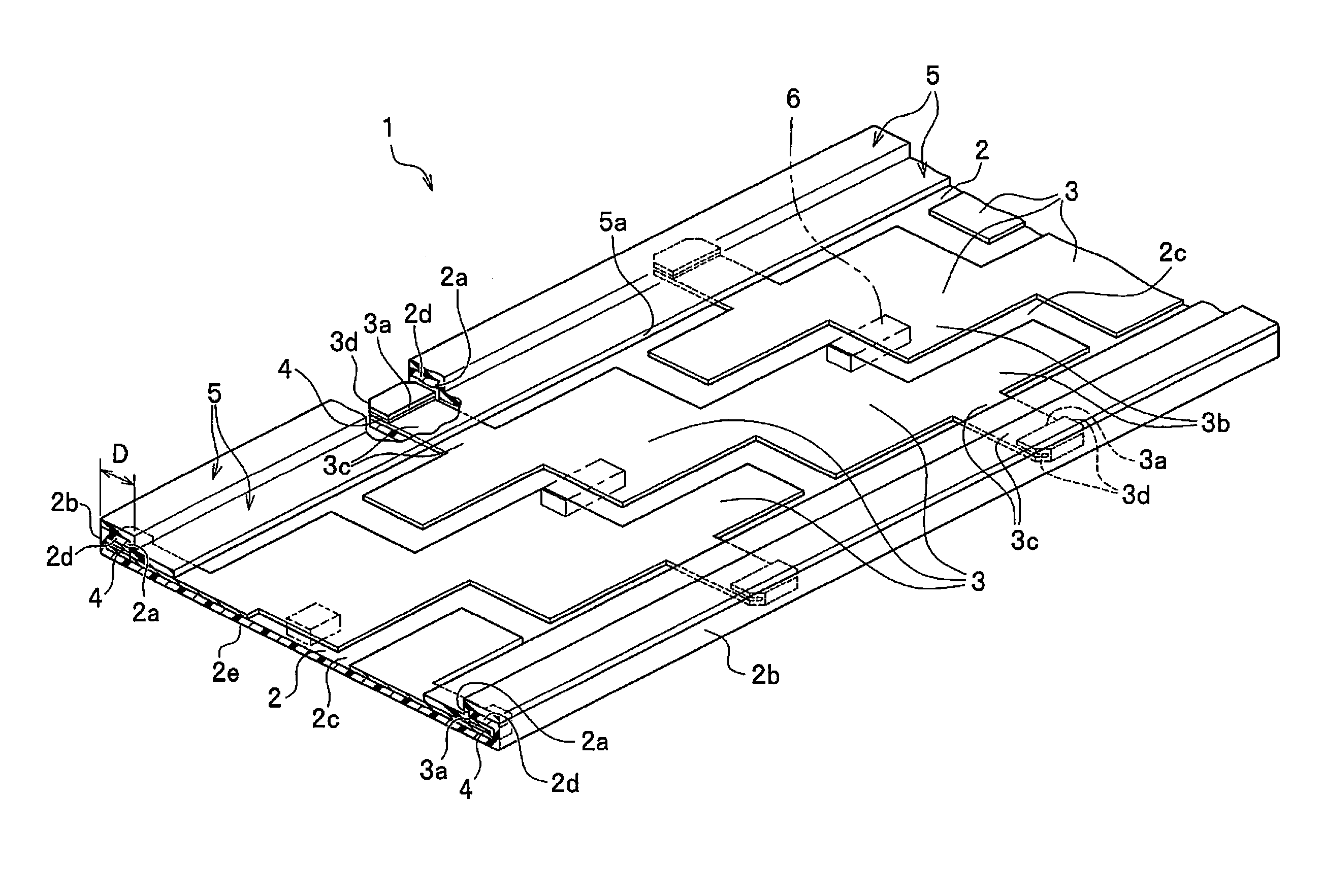
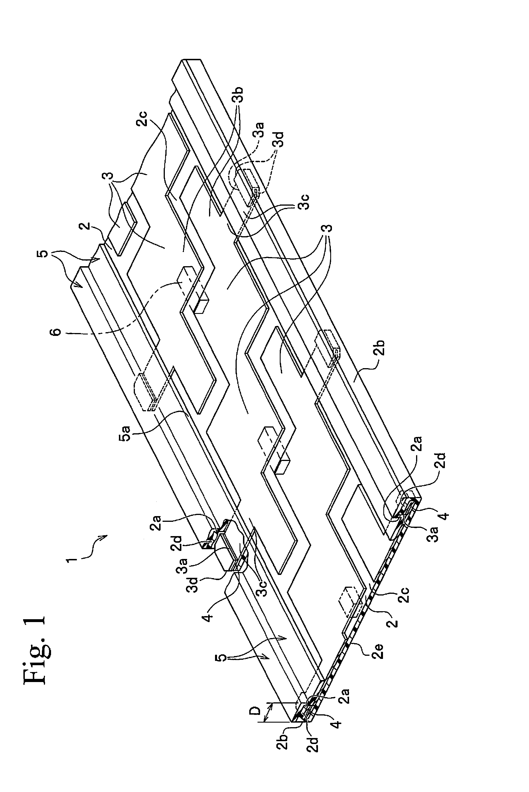
When the edge of the wiring pattern is exposed in the same plane as the end of the insulated board in the conventional flexible wiring board, the distance from the rear face side of the insulated board to the wiring pattern (called the creepage distance) may be extremely short.
Accordingly, with the flexible wiring board, if the light emitting element is mounted on the wiring pattern and housed in a housing, for example, there may be the problem that the drive power applied to the wiring pattern will flow through the edge of the wiring pattern to the metal housing and shock the user.
There may be also problems such as the fact that noise such as static electricity from the outside can passes to the metal housing through the edge of the wiring pattern, which creates uneven brightness in the light emitting element and makes it difficult to emit light in a stable state.

Method used


Image

  • Wiring board and light emitting device using same
  • Wiring board and light emitting device using same
  • Wiring board and light emitting device using same

Examples


first modification example

[0088]The present invention is not limited to or by the above embodiment, and various modifications and changes are possible within the technological scope of the present invention. The present invention also encompasses these modifications and changes. In the description below, the same designations or the same reference numerals may, in principle, denote the same or like members.

[0089]As shown in FIG. 6, in the above embodiment, a case in which the surface of the folded parts 2d formed by folding is coated with the resist 5 is described as an example of the resist 5, but this is not limited thereto.

[0090]As shown in FIGS. 8 to 10, a resist 50 (reflecting member) may be provided to the entire rear face 2e of the substrate 2, and the resist 50 that is on the rear face 2e side of the substrate 2 before the folded parts 2d are formed may be disposed on the upper face 2c side of the substrate 2 when the bending lines L is bent toward the upper face 2c of the substrate 2 to form the fol...

modification examples

Other Modification Examples

[0093]In the above embodiment, a light emitting device S that is used for a liquid crystal backlight, in which the wiring board 1 is bonded to the housing Sc in a state of being disposed flat is described. However, the light emitting device S can be given a shape corresponding to a straight fluorescent tube by housing the narrow and long, rectangular wiring board 1 in a translucent case or cover.

[0094]If the flexible wiring board 1 is bent in a circular shape in side view (with the upper face 2c on the outer peripheral side), and housed in a cover member Sb or housing Sc that is formed in an annular shape (doughnut shape), it is possible to obtain a lighting device with a shape corresponding to a round fluorescent tube.

[0095]Because the wiring board 1 can be bent, the light emitting device S can be changed to a device of a variety of shapes by bending the wiring board 1 in an arc shape, a V shape, a U shape, a semicircular shape, or the like, and housing i...


PUM


Abstract

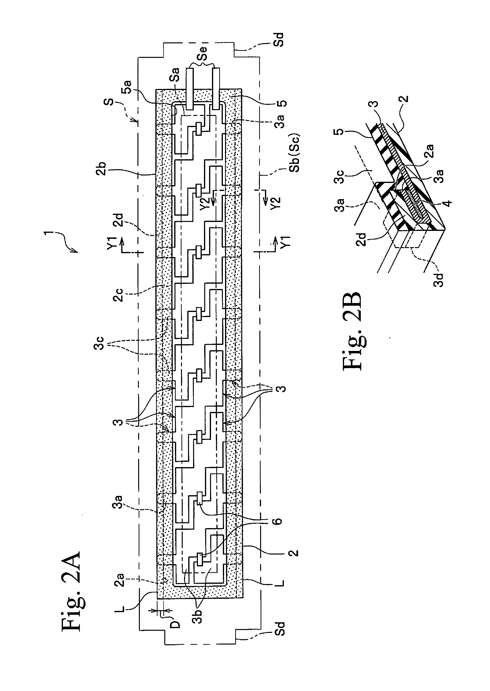
A wiring board includes an insulated substrate, a wiring pattern and a folded part. The insulated substrate has an elongated shape with shorter sides extending along a width direction. The wiring pattern is provided on the substrate. The wiring pattern extends between both ends in the width direction of the substrate, and has an exposed part exposed at at least one of the ends of the substrate. In the folded part, the exposed part of the wiring pattern and the substrate are integrally folded up inwardly toward an upper face side of the substrate at each of the ends of the substrate.

Description

CROSS-REFERENCE TO RELATED APPLICATIONS[0001]This application claims priority to Japanese Patent Application No. 2013-100696 filed on May 10, 2013. The entire disclosure of Japanese Patent Application No. 2013-100696 is hereby incorporated herein by reference.BACKGROUND[0002]The present disclosure relates to a wiring board comprising, for example, a flexible insulated substrate and a wiring pattern provided on the substrate, as well as to a light emitting device in which this wiring board is used.Description of the Related Art[0003]In order to perform plating on a wiring pattern of a flexible wiring board for light emitting device, the flexible wiring board has a connecting pad for connecting an electroplating electrode, and is connected to a wiring pattern.[0004]The flexible wiring board is usually made by forming a single continuously formed wiring pattern, and then being cut at a specific location, so a wiring conductor is exposed at the cut part (see JP H6-6003A, for example).[0...

Claims


Application Information

Patent Timeline
IPC IPC(8): H05K1/02F21V23/00
CPCH05K1/0298F21V23/00H05K2201/09009H05K1/028H05K2201/055H05K2201/09727H05K2201/10106F21Y2103/10F21Y2115/10H05K1/0256
Inventor MIYATA, TADAAKI
Owner NICHIA CORP
Learn More