Sold-state imaging device and electronic apparatus
Active Publication Date: 2014-11-27
SONY CORP
View PDF6 Cites 29 Cited by
- Summary
- Abstract
- Description
- Claims
- Application Information
AI Technical Summary
Benefits of technology
The patent is about a new type of solid-state imaging device that has a trench element isolation area that is offset from the edges of the pixels. This means that the position and volume of the device can be controlled based on the wavelength of light received by each pixel, resulting in improved color balance between different wavelengths of light. This allows for capture of images with good color balance and improved imaging properties without color distortion.
Problems solved by technology
Even in a solid-state imaging device having a configuration in which a trench element isolation area is provided in a semiconductor substrate, however, the collapse of color balance occurs that depends on a wavelength of received light and an incidence angle of the received light, which is a factor to cause coloring.
Method used
View moreImage
Smart ImageViewing Examples

Examples
first embodiment (
2. First Embodiment (First Example in which Position of Trench Element Isolation Area is Displaced to Side of Pixel of Long-wavelength)
second embodiment (
3. Second Embodiment (Second Example in which Position of Trench Element Isolation Area is Displaced to Side of Pixel of Long-wavelength)
third embodiment (
4. Third Embodiment (Third Example in which Position of Trench Element Isolation Area is Displaced to Side of Pixel of Long-wavelength)
Login to View More PUM
 Abstract
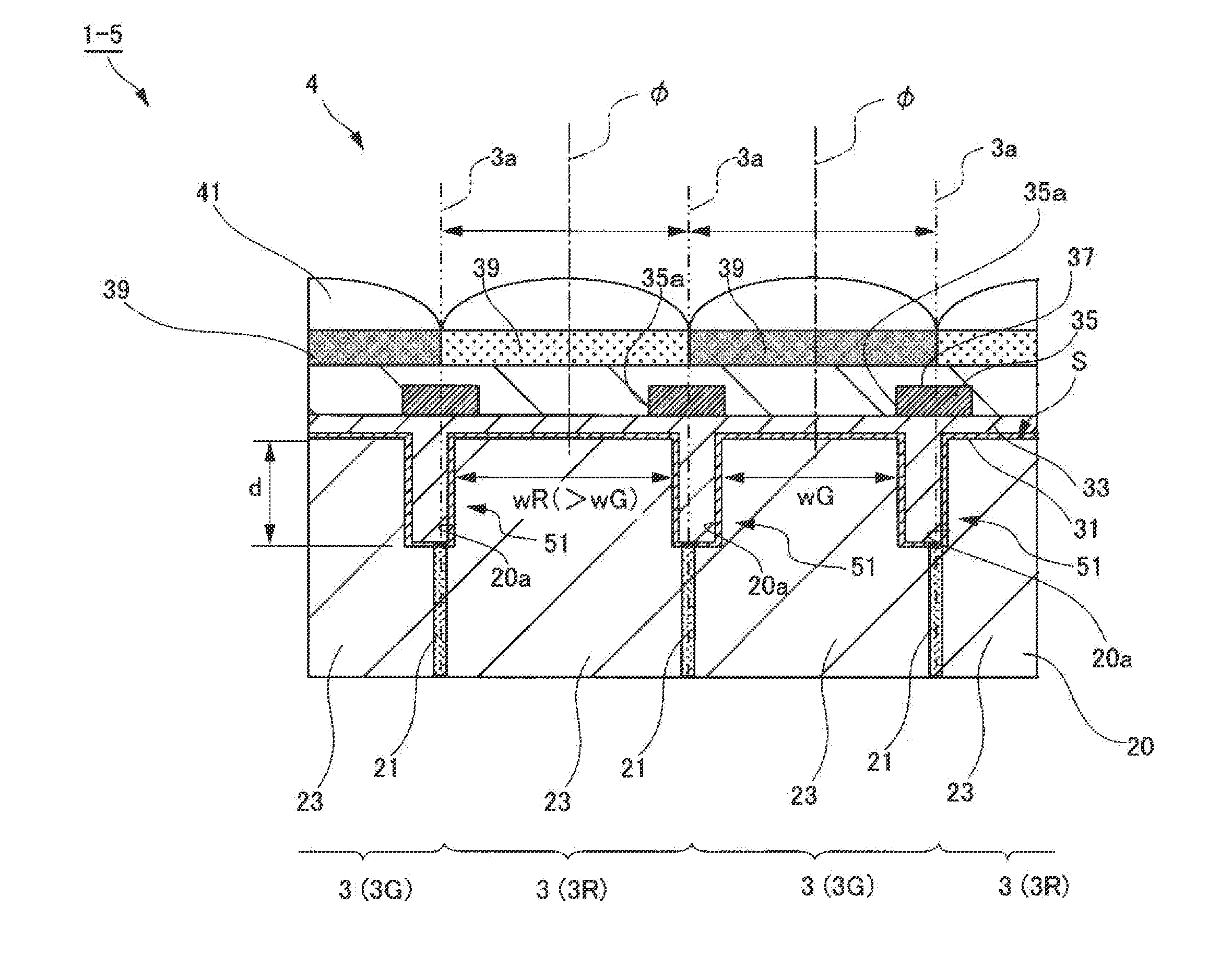
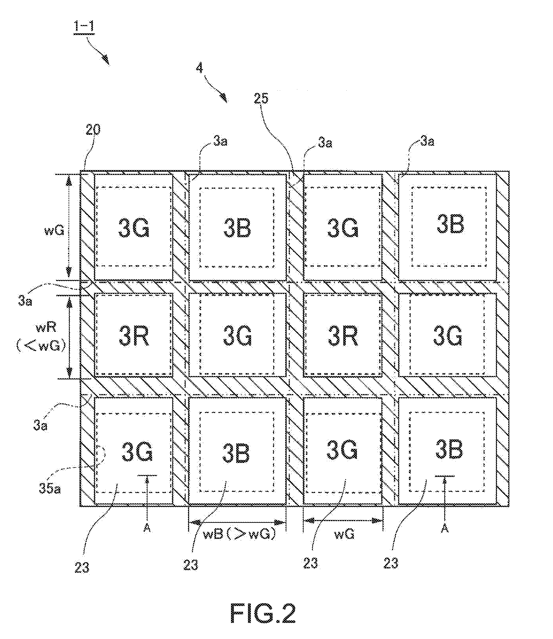
A solid-state imaging device includes a semiconductor layer on which a plurality of pixels are arranged along a light-receiving surface being a main surface of the semiconductor layer, photoelectric conversion units provided for the respective pixels in the semiconductor layer, and a trench element isolation area formed by providing an insulating layer in a trench pattern formed on a light-receiving surface side of the semiconductor layer, the trench element isolation area being provided at a position displaced from a pixel boundary between the pixels.
Description
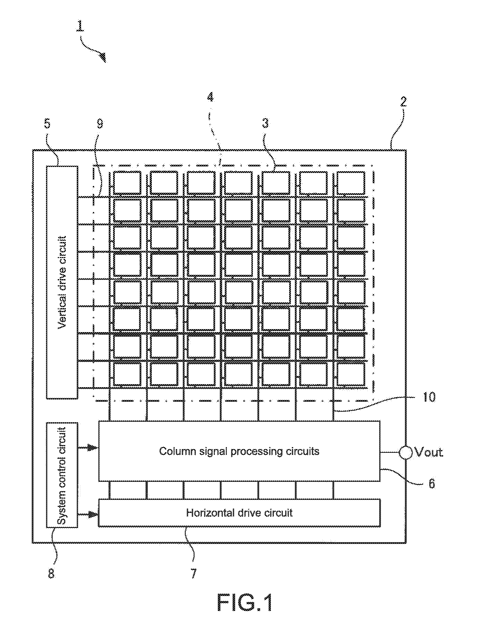
CROSS REFERENCE TO RELATED APPLICATIONS[0001]This application claims the benefit of Japanese Priority Patent Application JP 2013-109636 filed May 24, 2013, the entire contents of which are incorporated herein by reference.BACKGROUND[0002]The present disclosure relates to a solid-state imaging device and an electronic apparatus, and particularly to a solid-state imaging device including a trench element separation area and an electronic apparatus including the solid-state imaging device.[0003]A solid-state imaging device includes a plurality of pixels arranged along a light-receiving surface side of a semiconductor substrate. The respective pixels include a photoelectric conversion unit provided in the semiconductor substrate, and a color filter and an on-chip lens provided on the upper side of the semiconductor substrate.[0004]In the solid-state imaging device having such a configuration, if light that has obliquely entered a light-receiving surface leaks to a photoelectric conversi...
Claims
Login to View More Application Information
Patent Timeline
 IPC IPC(8): H01L27/146
CPCH01L27/14623H01L27/14627H01L27/14621H01L27/1463H01L27/14645H01L27/14629H01L27/14636H01L27/14656
Inventor OKAZAKI, HIROMI
Owner SONY CORP
Features
- R&D
- Intellectual Property
- Life Sciences
- Materials
- Tech Scout
- Unparalleled Data Quality
- Higher Quality Content
- 60% Fewer Hallucinations
Learn More Browse by: Latest US Patents, China's latest patents, Technical Efficacy Thesaurus, Application Domain, Technology Topic, Popular Technical Reports.
© 2025 PatSnap. All rights reserved.Legal|Privacy policy|Modern Slavery Act Transparency Statement|Sitemap|About US| Contact US: help@patsnap.com