Semiconductor devices and methods of fabrication with reduced gate and contact resistances

a technology of semiconductor devices and contact resistances, which is applied in the direction of semiconductor devices, semiconductor/solid-state device details, electrical apparatus, etc., can solve the problems of undesirable changes in gate and/or contact resistance, and the performance characteristics of transistors

Active Publication Date: 2014-12-04
GLOBALFOUNDRIES US INC +1
View PDF1 Cites 56 Cited by
  • Summary
  • Abstract
  • Description
  • Claims
  • Application Information

AI Technical Summary

Problems solved by technology

This ever-decreasing transistor size can result in challenges to the performance characteristics ...

Method used


Image

  • Semiconductor devices and methods of fabrication with reduced gate and contact resistances
  • Semiconductor devices and methods of fabrication with reduced gate and contact resistances
  • Semiconductor devices and methods of fabrication with reduced gate and contact resistances

Examples


Embodiment Construction

[0026]Aspects of the present invention and certain features, advantages, and details thereof, are explained more fully below with reference to the non-limiting examples illustrated in the accompanying drawings. Descriptions of well-known materials, fabrication tools, processing techniques, etc, are omitted so as not to unnecessarily obscure the invention in detail. It should be understood, however, that the detailed description and the specific examples, while indicating aspects of the invention, are given by way of illustration only, and are not by way of limitation. Various substitutions, modifications, additions, and / or arrangements, within the spirit and / or scope of the underlying inventive concepts will be apparent to those skilled in the art from this disclosure.

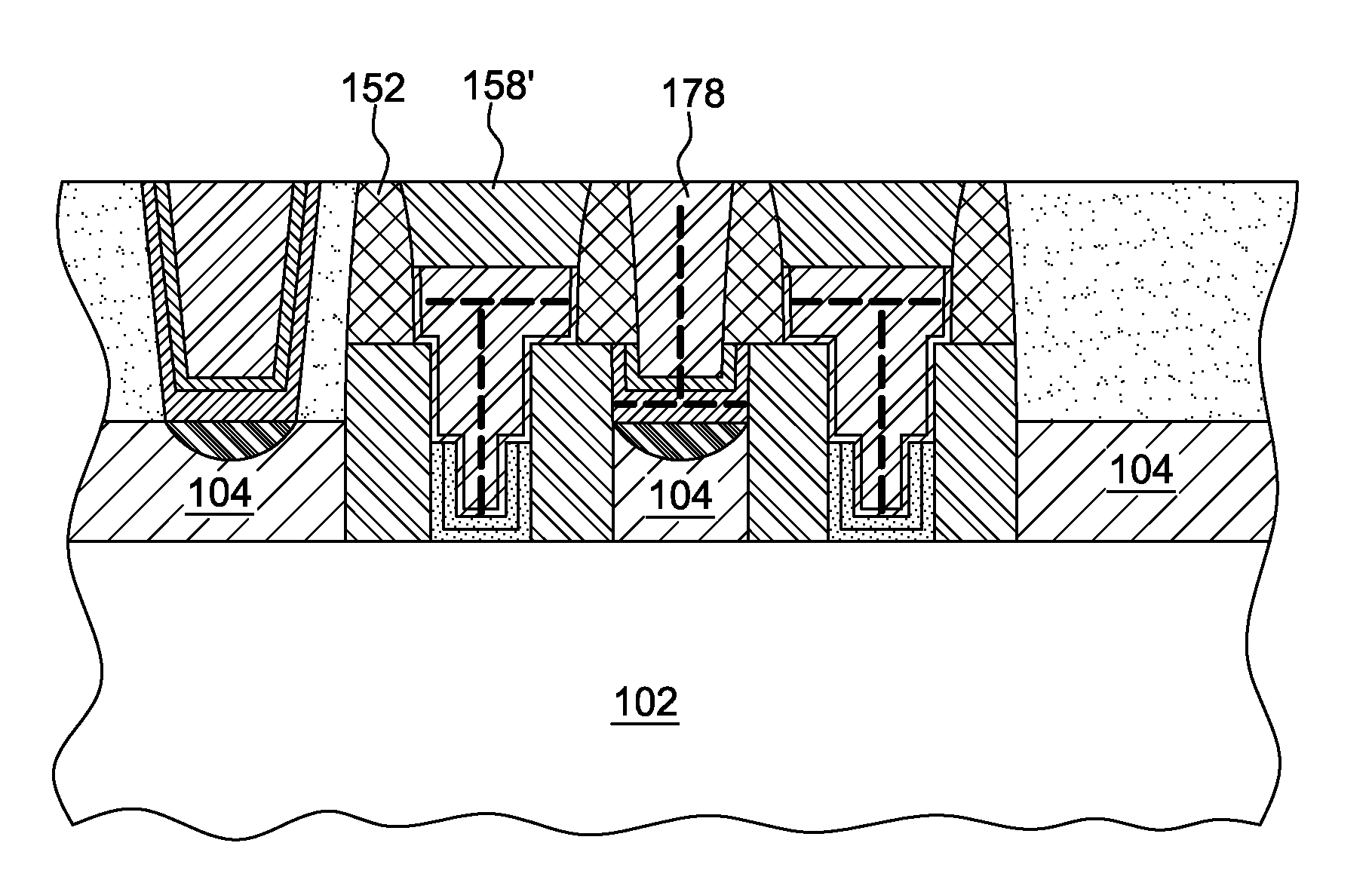
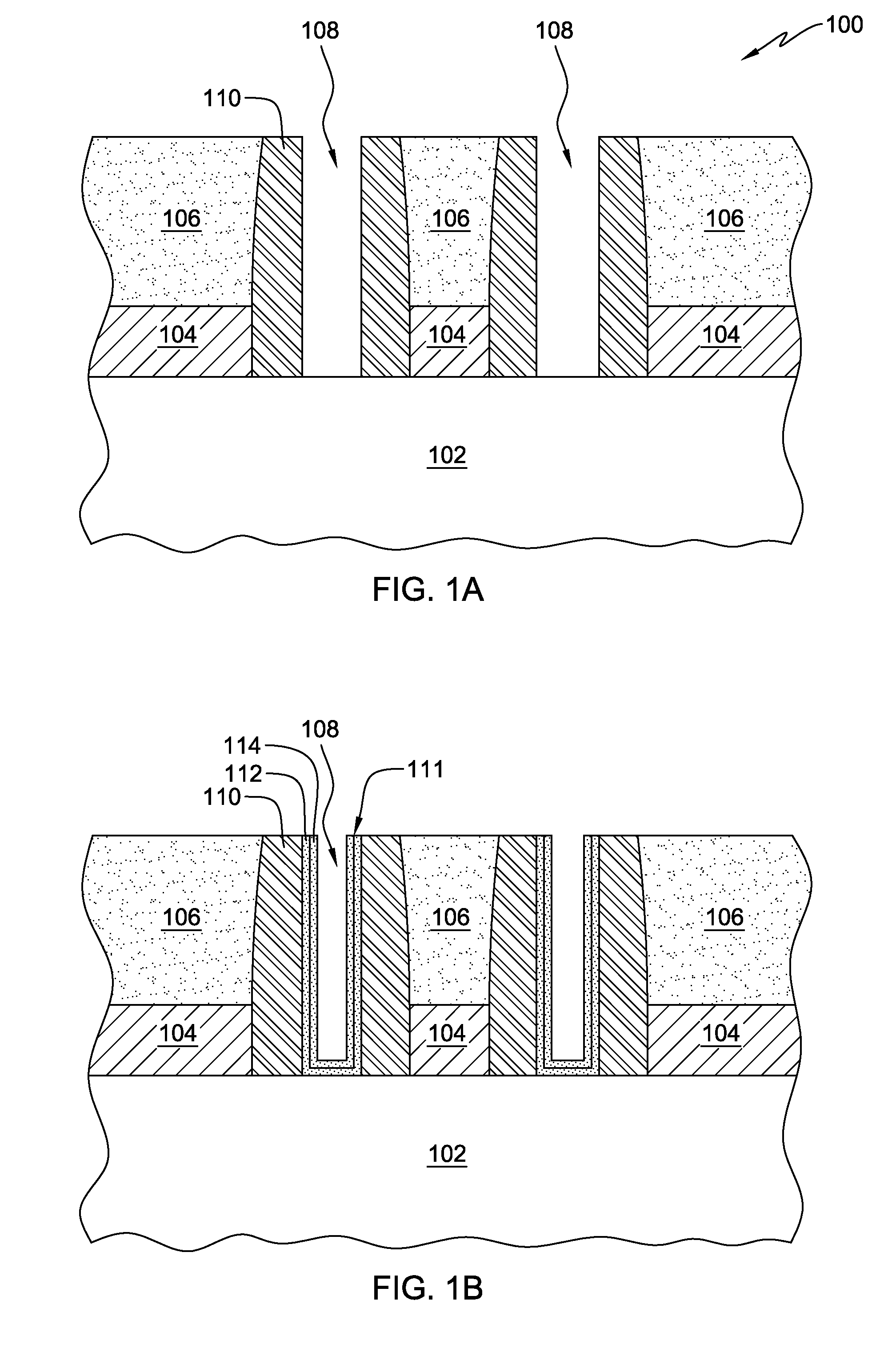
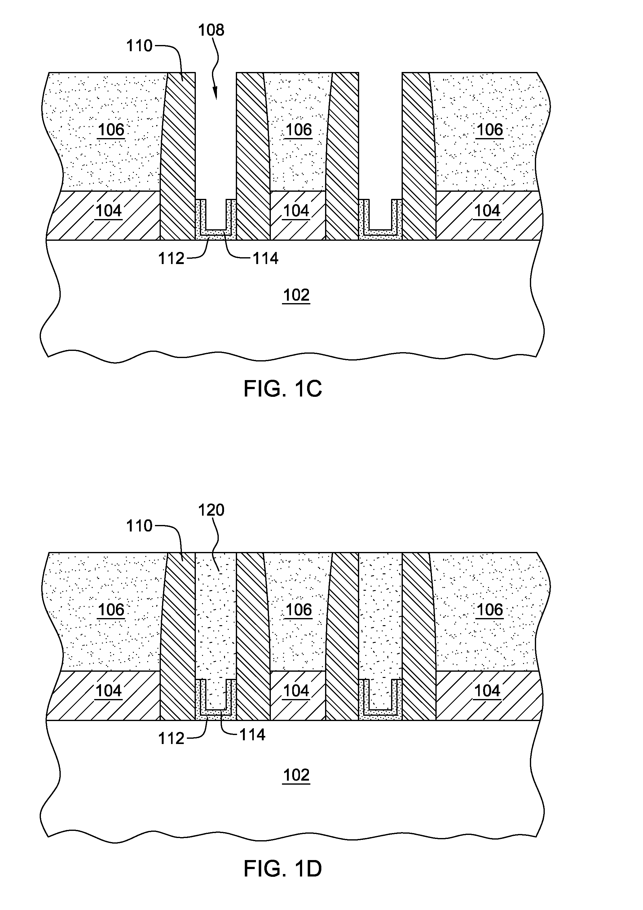
[0027]In one aspect, semiconductor device fabrication typically includes transistor formation processing, which may involve conductive material deposition into appropriately configured openings in an intermediate circu...


PUM


Abstract

Semiconductor structures with reduced gate and/or contact resistances and fabrication methods are provided. The method includes: providing a semiconductor device, which includes forming a transistor of the semiconductor device, where the transistor forming includes: forming a T-shaped gate for the transistor, the T-shaped gate being T-shaped in elevational cross-section; and forming an inverted-T-shaped contact to an active region of the transistor, the inverted-T-shaped contact including a conductive structure with an inverted T-shape in elevational cross-section.

Description

FIELD OF THE INVENTION[0001]The present invention relates in general to semiconductor devices and methods of fabricating semiconductor devices, and more particularly, to transistor structures with reduced gate and / or contact resistances, and methods of fabrication thereof.BACKGROUND OF THE INVENTION[0002]As is known, semiconductor devices, such as integrated circuit devices, typically include a large number of transistors within a single chip or wafer area. As integration density of transistors continues to increase, the footprint area occupied by individual transistors necessarily continues to decrease. This ever-decreasing transistor size can result in challenges to the performance characteristics of the transistors, including (for instance) undesirable changes to the gate and / or contact resistances.BRIEF SUMMARY[0003]The shortcomings of the prior art are overcome, and additional advantages are provided through the provision, in one aspect, of a method which includes providing a s...

Claims


Application Information

Patent Timeline
IPC IPC(8): H01L21/28H01L29/417H01L29/423H01L21/283
CPCH01L21/28008H01L29/42376H01L29/41775H01L21/283H01L21/28088H01L21/28114H01L21/76834H01L21/76843H01L21/76885H01L21/76897H01L21/823425H01L21/823475H01L23/485H01L23/53266H01L29/665H01L29/6653H01L29/66545H01L29/66628H01L2924/0002H01L2924/00
Inventor XIE, RUILONGCAI, XIUYUKAMINENI, VIMALCHENG, KANGGUOKHAKIFIROOZ, ALI
Owner GLOBALFOUNDRIES US INC
Why Eureka
Try Eureka