Method For Modulating A Micro-Led Display

a micro-led display and modulation scheme technology, applied in the field of digital displays, can solve the problems of the continued decline of the led system, and achieve the effect of improving modulation efficiency and gray scale modulation

Inactive Publication Date: 2014-12-18
JASPER DISPLAY
View PDF6 Cites 9 Cited by
  • Summary
  • Abstract
  • Description
  • Claims
  • Application Information

AI Technical Summary

Benefits of technology

[0004]The present invention provides methods, systems, and apparatus for improved gray scale modulation. More specifically, the present invention uses spacing of row write actions on a display to create gray scale modulation. In one embodiment, a scheme is provided for modulating a micro-LED display by use of a system of write pointers to cause the modulation of rows to result in the generation of gray scale on the image. The present invention is based in part on the principle that a row-write function establishes a gray scale modulation state that remains in place until a new set of gray scale data is written to that same row. By controlling the writing of new data states, gray scale modulation may be achieved. Additionally, the present invention may deal with each row individually. Improved modulation efficiency may allow the use of lower frequency imaging circuits to achieve the same display image. At least some of these and other objectives described herein will be met by some embodiments of the present invention.

Problems solved by technology

As the cost of LED systems continues to fall, it is predicted that they will eventually take over the market for LCD applications.

Method used


Image

  • Method For Modulating A Micro-Led Display
  • Method For Modulating A Micro-Led Display
  • Method For Modulating A Micro-Led Display

Examples


Embodiment Construction

[0035]It is to be understood that both the foregoing general description and the following detailed description are exemplary and explanatory only and are not restrictive of the invention, as claimed. It should be noted that, as used in the specification and the appended claims, the singular forms “a”, “an” and “the” include plural referents unless the context clearly dictates otherwise. Thus, for example, reference to “a material” may include mixtures of materials; reference to “a display” may include multiple displays, and the like. References cited herein are hereby incorporated by reference in their entirety, except to the extent that they conflict with teachings explicitly set forth in this specification.

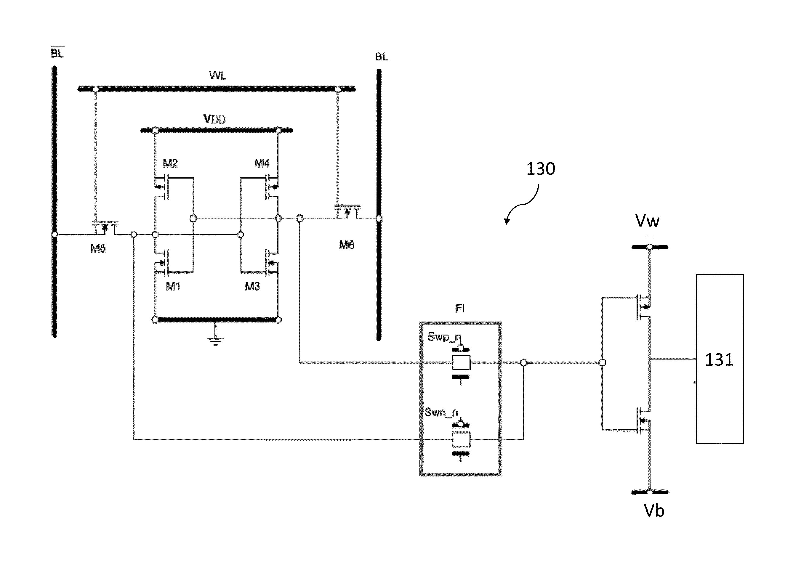
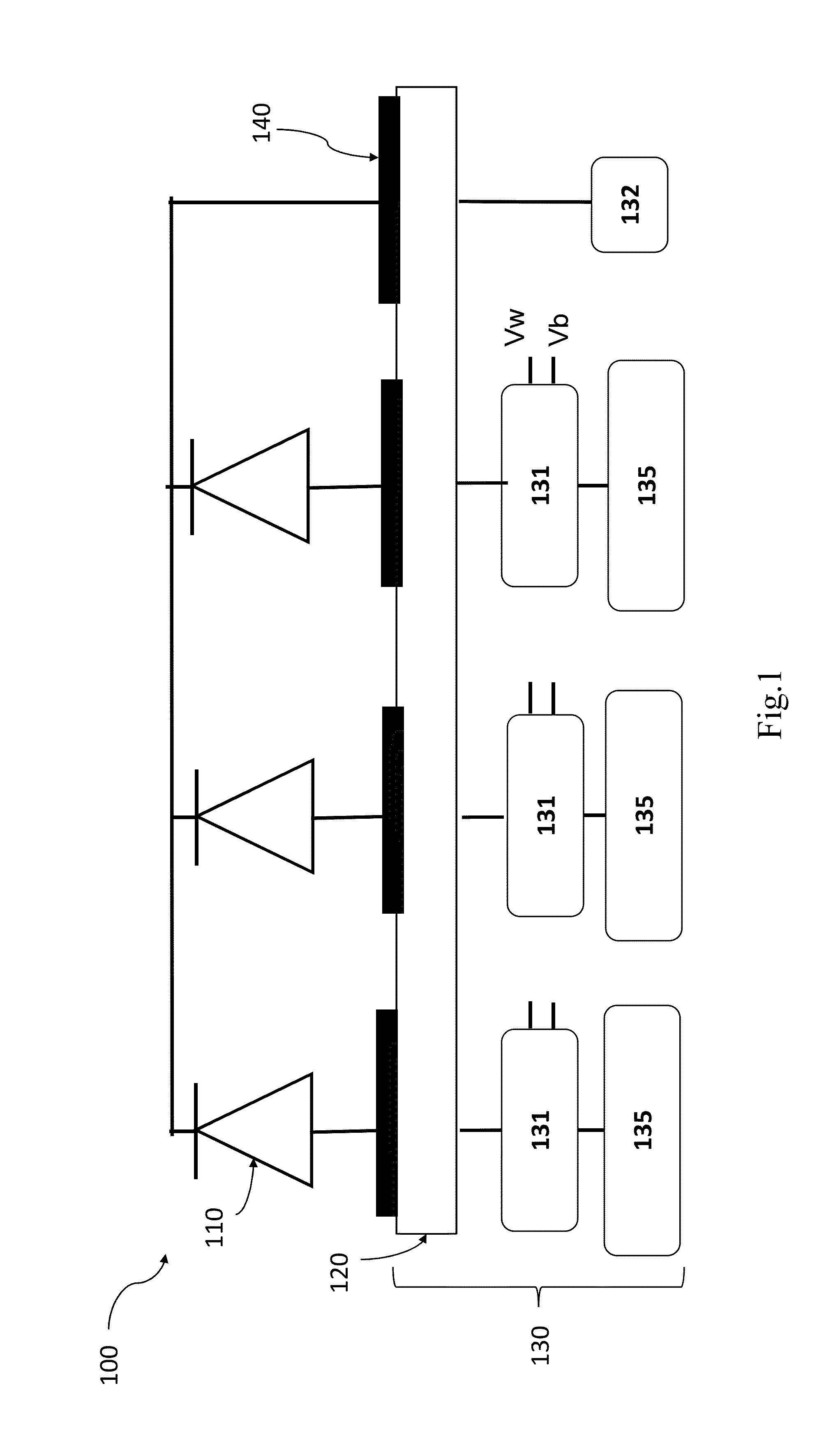
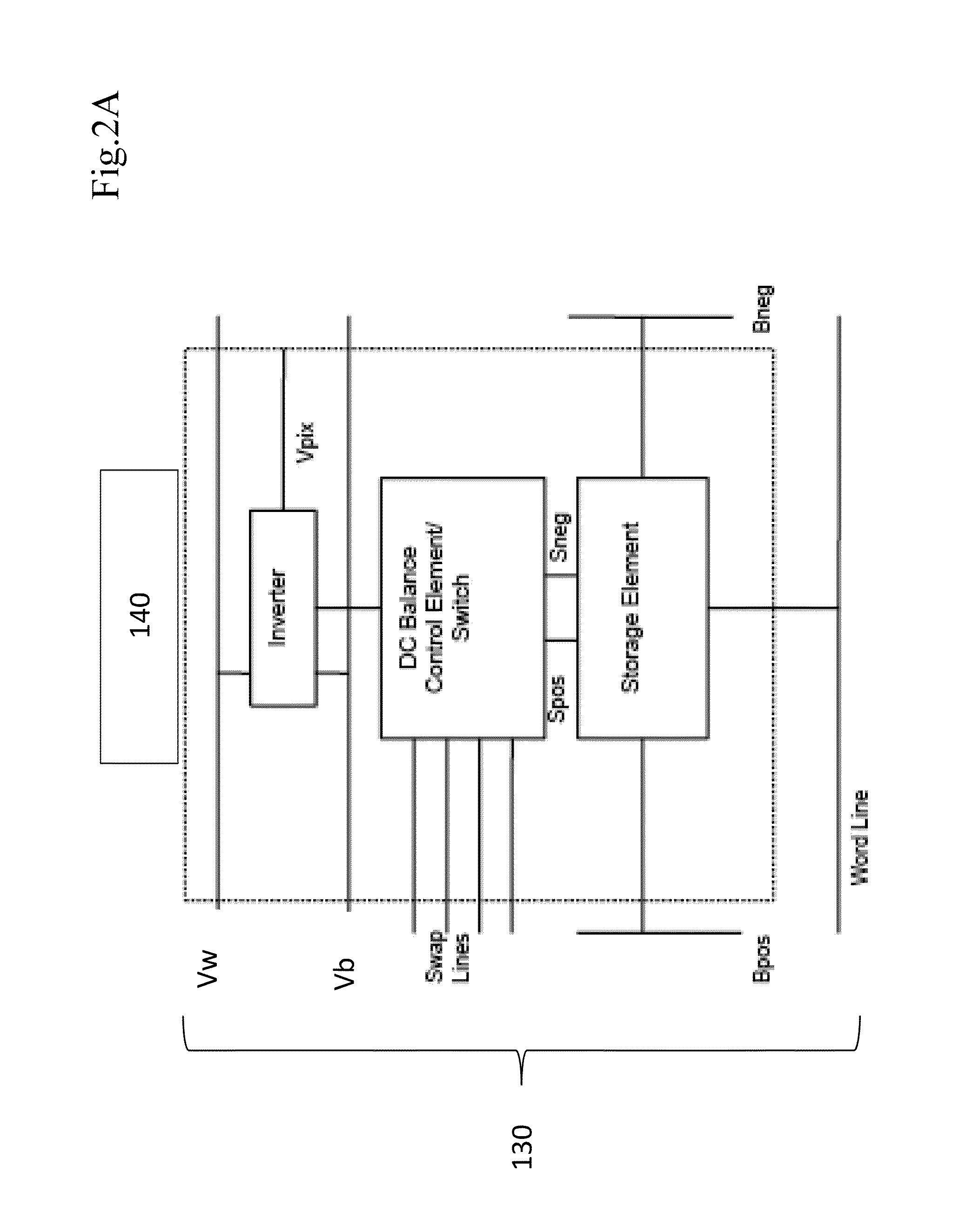
[0036]In the following description we will make use of the term “write pointer”. A write pointer points to a row on the display which has a particular row spacing relationship to the rows below and above it which are also pointed to by write pointers. The locations of a set of ...


PUM


Abstract

A micro-LED display device and modulation scheme for applying image data to an imager. The micro-LED display, including a plurality of micro-LED pixels disposed in rows and columns array, may use a modulation scheme. The method includes using row write actions to write data to said rows of micro-LED pixels; and using spacing of row write actions to create grey scale modulation, wherein one spacing between sequential row write actions is at a first distance while another spacing between sequential row write actions is at a second distance greater than said first distance.

Description

CROSS-REFERENCE TO RELATED APPLICATIONS[0001]This application is a Continuation-in-Part of U.S. patent application Ser. No. 13 / 790,120, “MODULATION SCHEME FOR DRIVING DIGITAL DISPLAY SYSTEMS”, filed Mar. 8, 2013, and also claims the benefit of priority to U.S. provisional patent application Ser. No. 61 / 835,724 entitled “MICROLED ON SILICON”, filed Jun. 15, 2013, which is also incorporated herein by reference.FIELD OF THE INVENTION[0002]The present invention pertains to digital displays, and more particularly, to modulation schemes for driving micro-LED displays.BACKGROUND OF THE INVENTION[0003]Light emitting diode (LED) display technology has progressed in recent years, and has become an increasingly common option for display systems, currently making up the largest portion of the flat panel display market. This market dominance is expected to continue into the future. The superior characteristics of LED display with regard to weight, power, and geometry in image visualization, have...

Claims


Application Information

Patent Timeline
Patent Type & Authority Applications(United States)
IPC IPC(8): G09G3/20G09G3/32
CPCG09G3/2014G09G3/32G09G2320/0271G09G2320/0252G09G2300/0857
Inventor LIAO, CHENG-HSINGTSAI, CHIA-JENHUDSON, EDWIN LYLEMCDONALD, DAVID CHARLESCOWL, DAVID JOHN
Owner JASPER DISPLAY
Why Eureka
Try Eureka