Power supply control device, semiconductor device and method of driving semiconductor device
Inactive Publication Date: 2005-08-02
SONY CORP
View PDF22 Cites 43 Cited by
Summary
Abstract
Description
Claims
Application Information
AI Technical Summary
This helps you quickly interpret patents by identifying the three key elements:
Problems solved by technology
Method used
Benefits of technology
Benefits of technology
[0037]A first object of the present invention is to provide a power supply voltage control apparatus carrying an input signal generation circuit having a high general use which is able to be commonly used for monitor circuits having various delays suitable for different types of semiconductor circuits and which can be used for a monitor circuit capable of being changed in delay by electrical control.
[0039]A third object of the present invention is to provide a power supply voltage control apparatus able to raise the stability of operation of a semiconductor circuit without impeding the effect of reducing the power consumption.
[0040]A fourth object of the present invention is to provide a semiconductor device keeping the increase of circuit scale to a minimum and enabling more flexible and efficient design and a method for driving the same.
[0051]In this way, since the delay of the reference signal from an input signal generation circuit can be changed to an optimal value to enable detection of delay, detection of delay is possible for monitor circuits having various delay values designed in accordance with the type of semiconductor circuit. When a detection result is output from the delay detection circuit, the power supply voltage to be supplied to the semiconductor circuit and monitor circuit from the power supply voltage control circuit is changed or maintained accordingly.
[0055]According to the power supply voltage control apparatus according to the second aspect, the built-in monitor circuit is designed so that a delay characteristic similar to the delay characteristic of the critical path of a semiconductor circuit can be obtained. Namely, in the past, a monitor circuit was designed so that the same element configuration as the critical path could be reproduced, but in the power supply voltage control apparatus of the present invention, it is enough if a similar type delay characteristic having an absolute value of the delay and a change of the delay value relative to the power supply voltage smaller than those of the critical path by a constant ratio is obtained. Therefore, it is not necessarily required to provide the same element configuration as with the critical path. For example, it is possible to adopt a circuit configuration in which the absolute value of the delay is made half that of the critical path while maintaining a ratio of the wiring delay component and the gate delay component forming the absolute value of the delay the same. In this case, since the absolute value of the delay is half, it is possible to reduce the number of elements, reduce the element sizes, and shorten the wiring accordingly.
[0091]Due to this, different delay component characteristics are combined, it is possible to more closely approach the configuration of the critical path of the target circuit, and it becomes possible to keep to a minimum the increase in the size of the circuit due to the provision of a plurality of delay elements having different delay characteristics.
Problems solved by technology
As a result, this had become one factor increasing the burden in design and development of power supply voltage control apparatuses.
Therefore, when the delay value of the critical path of an LSI was large, the conventional monitor circuit for reproducing the delay characteristic included a large number of gate elements etc. and became large in size.
Therefore, if the area of the power supply voltage control apparatus was large and this apparatus was integrated into an LSI, the cost of the LSI ended up rising.
Further, in the above power supply voltage control apparatus, for example, the output of a DC—DC converter or other source for supplying the power supply voltage sometimes fluctuates for a very short time because of noise etc.
If the margin of the power supply voltage is made too large, however, the inherent effect of the power supply voltage control apparatus, that is, to supply the minimum limit of power supply voltage required so as to reduce the power consumption, ends up being weakened.
However, in the former method in which the critical path of the target circuit itself is extracted for configuration, it is extremely difficult to extract a complicated critical path from a target circuit itself by path analysis.
The critical path extracted by such work does not always match the critical path of a target circuit actually formed.
In addition, work of extracting a critical path from the massive results of path analysis results is liable to lead to a longer design period.
Further, in the method in which a multistage string of delay elements is used for configuration, the strings of delay elements cannot always reproduce the critical path of the target circuit.
Further, if preparing a plurality of multistage strings of delay elements differing in characteristics, the size of the circuit increases.
Method used
Image
Click on the blue label to locate the original text in one second.
Reading with bidirectional positioning of images and text.
Examples
first embodiment
[0121
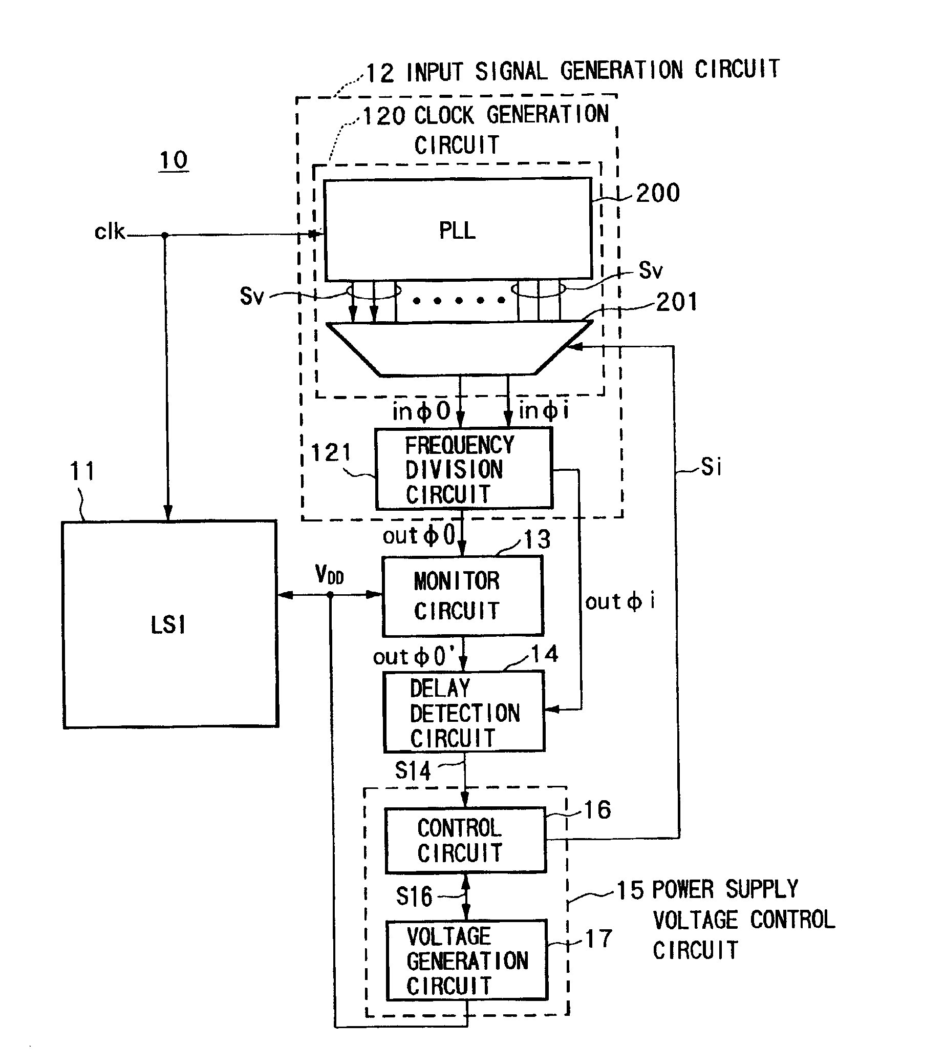
[0122]FIG. 1 is a block diagram of an embodiment of a power supply voltage control apparatus according to the present invention.
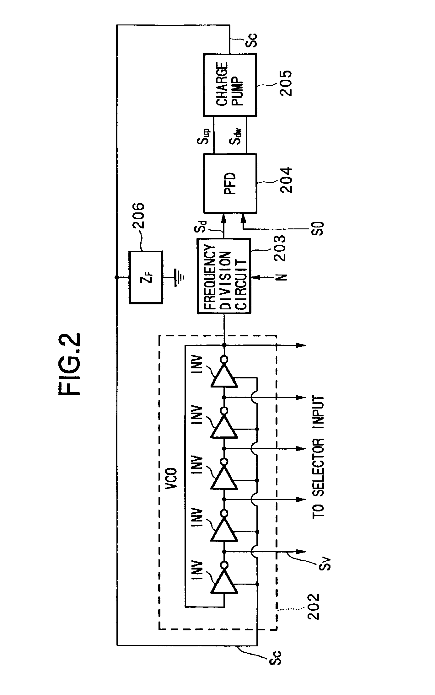
[0123]The power supply voltage control apparatus 10 includes a semiconductor circuit 11 (LSI) serving as a target circuit supplied with a controlled power supply voltage VDD, an input signal generation circuit 12, a monitor circuit 13 for monitoring the delay characteristic of the critical path of the LSI 11, a delay detection circuit 14, and a power supply voltage control circuit 15. The power supply voltage control circuit 15 has a control circuit 16 and a voltage generation circuit 17.
[0124]Together with the semiconductor circuit 11, the input signal generation circuit 12, the monitor circuit 13, and the delay detection circuit 14 are integrated on a single chip. The power supply voltage control circuit 15 may be integrated in the same chip as the LSI or in another LSI.
[0125]The semiconductor circuit 11 is supplied with the power supply voltage VDD ...
second embodiment
[0179
[0180]The second embodiment relates to the change of the delay characteristic of a monitor circuit. Therefore, the configurations and basic operations of the parts of the power supply voltage control apparatus are the same as those of the first embodiment. FIG. 1 to FIG. 4 and FIGS. 5A to 5F are applied as they are.
[0181]In the above first embodiment, the characteristic between a power supply voltage and delay of the monitor circuit 13 was set to be equivalent to that of the critical path of the semiconductor circuit (LSI) 11.
[0182]As opposed to this, in the second embodiment, the monitor circuit 13 is given a characteristic between a power supply voltage and delay similar to that of the critical path. Here, “a characteristic between a power supply voltage and delay similar to that of the critical path” means a delay characteristic outputting a delayed signal having an absolute value of the delay and a change of the delay relative to the power supply voltage smaller than or lar...
third embodiment
[0196
[0197]FIG. 7 is a block diagram of another embodiment of the power supply voltage control apparatus according to the present invention.
[0198]The power supply voltage control apparatus 20 includes a semiconductor circuit 21 (LSI) supplied with a controlled power supply voltage VDD, a pulse generation circuit 22, a monitor circuit 23 for monitoring the delay characteristic of the critical path of the LSI 21, a delay element chain type delay detection circuit 24, and a power supply voltage control circuit 25. The power supply voltage control circuit 25 has a control circuit 26 and a power supply voltage generation circuit 27.
[0199]The semiconductor circuit 21 has the pulse generation circuit 22, the monitor circuit 23, and the delay detection circuit 24 integrated in it.
[0200]The semiconductor circuit 21 is supplied with the power supply voltage VDD by the power supply voltage generation circuit 27 and has a plurality of not shown transmission paths.
[0201]Each transmission path, f...
PUM
Abstract
A power supply voltage control apparatus including an input signal generation circuit of wide uses or a small-sized monitor circuit of a novel configuration, and a semiconductor circuit and a method for driving the same, having a semiconductor circuit 11, an input signal generation circuit 12 able to change the phase difference i of a reference signal outφi and an input signal outφ0 in accordance with a control signal Si when generating the two signals from a clock, a monitor circuit 13 having a characteristic between a power supply voltage and delay the same as that of a critical path of the semiconductor circuit 11, propagating the input signal outφ0, and outputting a delayed signal outφ0′ to be delayed exactly by a time equivalent to a delay of the critical path (or smaller by a constant ratio), a delay detection circuit 14 for detecting a delay of the delayed signal outφ0′ relative to the reference signal outφi, and a power supply voltagecontrol circuit 15 for controlling a power supply voltage VDD supplied to the semiconductor device 11 and the monitor circuit 13 based on the detection result.
Description
TECHNICAL FIELD[0001]The present invention relates to a power supply voltage control apparatus including a monitor circuit for obtaining a delay characteristic of a critical path in a semiconductor circuit or other target circuit and a semiconductor device and method of driving the same.BACKGROUND ART[0002]To respond to demands for reducing the power consumption of semiconductor integrated circuits (LSI) in recent years, it has been proposed to control the power supply voltage dynamically to deal with the variability in operation frequencies of LSI's and processes and to supply the minimum limit of voltage enabling an LSI to operate normally.[0003]In a power supply voltage control apparatus adopting such a so-called variable power supply voltage controlsystem, as shown in FIG. 26, in order to monitor the delay time of a critical path of the LSI 1, for example, a monitor circuit having a characteristic between a power supply voltage and delay equivalent to that of the critical path ...
Claims
Application Information
Patent Timeline
Application Date:The date an application was filed.
Publication Date:The date a patent or application was officially published.
First Publication Date:The earliest publication date of a patent with the same application number.
Issue Date:Publication date of the patent grant document.
PCT Entry Date:The Entry date of PCT National Phase.
Estimated Expiry Date:The statutory expiry date of a patent right according to the Patent Law, and it is the longest term of protection that the patent right can achieve without the termination of the patent right due to other reasons(Term extension factor has been taken into account ).
Invalid Date:Actual expiry date is based on effective date or publication date of legal transaction data of invalid patent.

