
Display device and electronic apparatus have the same

Active Publication Date: 2009-04-23
JOLED INC
View PDF10 Cites 42 Cited by
  • Summary
  • Abstract
  • Description
  • Claims
  • Application Information

AI Technical Summary

Benefits of technology

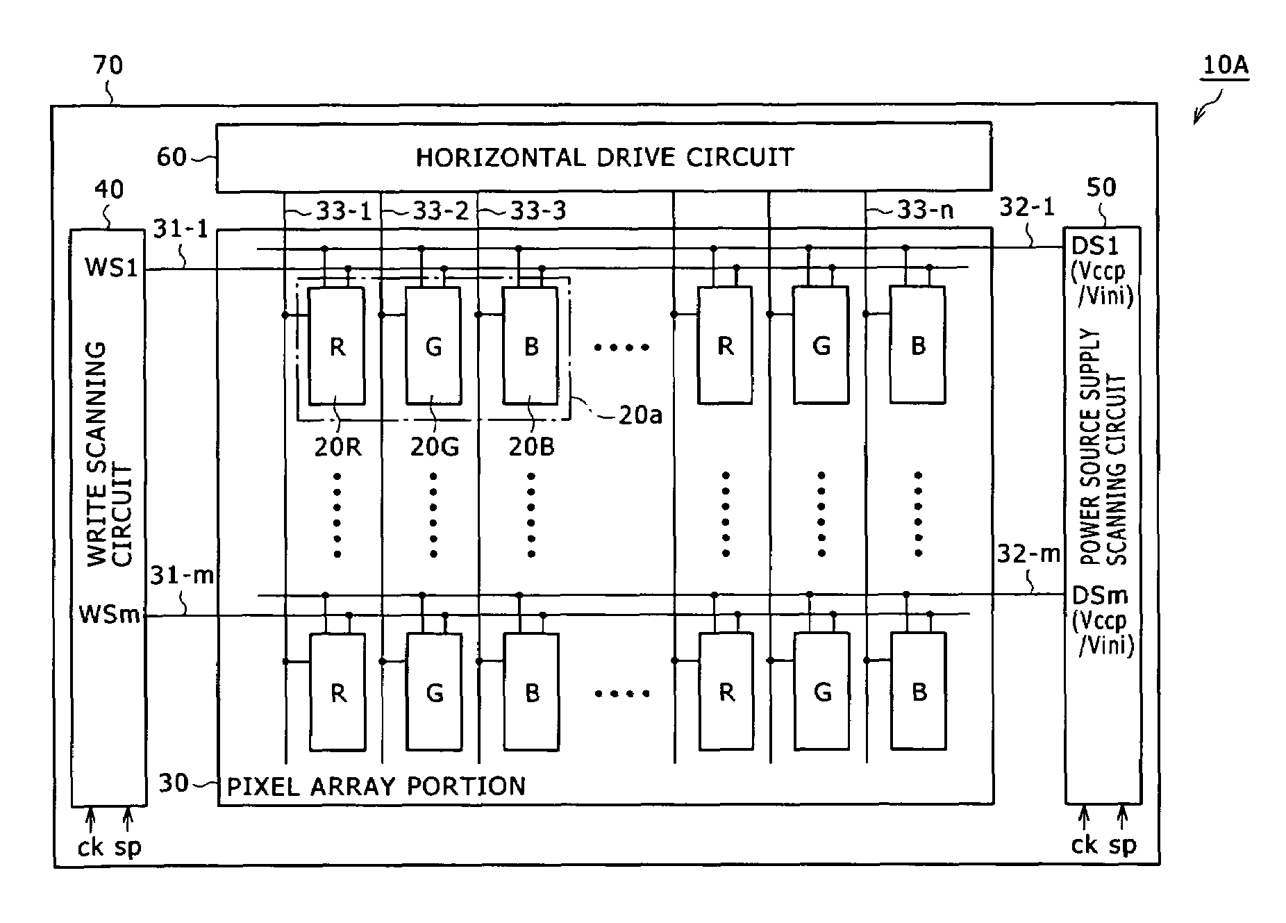
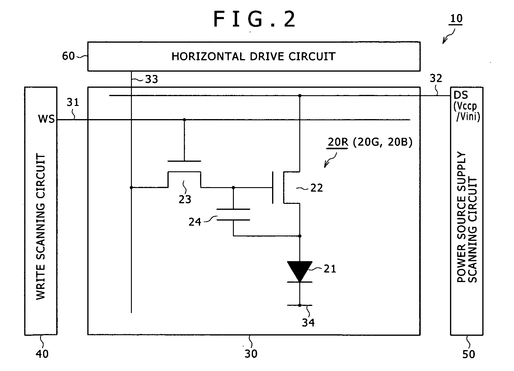
[0015]On the other hand, in order to reduce the number of elements and wirings constituting the pixel circuit, for example, it is expected to adopt a configuration with which a power source potential supplied to the drive transistor of the pixel circuit is made switchable. In this case, it is also expected to adopt a technique with which the drive transistor is given a function of controlling a time period for light emission / a time period for non-light emission of the organic EL element by switching the power source potential, thereby eliminating a dedicated transistor for controlling the light emission / the non-light emission.
[0021]When the number of power source supply lines is doubled, the degree of the high definition of the pixel is reduced because the power source supply lines have a large rate of occupation in the pixel area. In addition, when the number of power source supply lines is doubled, the number of stages of power source supply scanning circuits for driving the power source supply lines is also doubled. As a result, the circuit scale of the power source supply scanning circuits increases, thereby making it difficult to narrow a frame of a peripheral portion, of a pixel array portion, which is referred to as a so-called screen frame on a display panel.
[0025]In the display device having the configuration described above, and the electronic apparatus having the same, one power source supply line is made common to the plurality of adjacent sub-pixels constituting the same unit pixel and belonging to the plurality of rows. As a result, when the plurality of rows, for example, are two rows, that is, when the unit pixel is configured in units of two rows, it is possible to prevent occurrence of the case where the number of power source supply lines need to be doubled. In addition, the circuit configuration of the power source supply scanning circuit for driving the power source supply lines can be held as it is. As a result, it is possible to narrow the screen frame of the display panel. In addition, it is possible to realize the promotion of the high definition of the display panel because the size of each of the sub-pixels can be reduced.

Problems solved by technology

However, on the other hand, the number of elements constituting the pixel circuit is large, which impedes the miniaturization of the pixel size.

Method used


Image

  • Display device and electronic apparatus have the same
  • Display device and electronic apparatus have the same
  • Display device and electronic apparatus have the same

Examples


first example

[0152]FIG. 11 is a layout diagram showing a first example of a disposition relationship among the constituent elements of each of the sub-pixels of the unit pixel 20b, the scanning lines 31 and the power source supply line 32 in the case where one power source supply line 32 is wired every two rows. In the figure, constituent elements similar to or corresponding to those previously described with reference to FIG. 10 are designated with the same reference numerals, respectively.

[0153]As shown in FIG. 11, of the four kinds of sub-pixels 20W, 20R, 20G and 20B corresponding to W, R, G and B, respectively, for example, the sub-pixels 20W and 20B belong to the upper row, and the sub-pixels 20R and 20G belong to the lower row. In addition, the sub-pixels 20W and 20R belong to the left column, and the sub-pixels 20B and 20G belong to the right column.

[0154]In addition, as apparent from FIG. 11, the disposition of the constituent elements including the hold capacitor (Cs) 24 and the subsidi...

second example

[0159]FIG. 12 is a layout diagram showing a second example of a disposition relationship among the constituent elements of each of the sub-pixels of the unit pixel 20b, the scanning lines 31 and the power source supply line 32 in the case where one power source supply line 32 is wired every two rows. In the figure, constituent elements similar to or corresponding to those previously described with reference to FIG. 11 are designated with the same reference numerals, respectively.

[0160]The first example adopts the configuration that the wiring width 2×w2 of the power source supply line 32 is double the wiring width w2 in the case where one power source supply line 32 is wired every one row. On the other hand, as apparent from FIG. 12, the second example adopts a configuration that a wiring width w3 of the power source supply line 32 is set as being narrower than the wiring width 2×w2 in the first example.

[0161]Setting the wiring width w3 of the power source supply line 32 as being na...


PUM


Abstract

A display device includes a pixel array portion in which sub-pixels each including an electro-optic element, a write transistor for writing a video signal, a hold capacitor for holding the video signal written by the write transistor, and a drive transistor for driving the electro-optic element in accordance with the video signal held in the hold capacitor are disposed in a matrix, and each unit pixel is composed of the plurality of adjacent sub-pixels belonging to a plurality of rows. The display device further includes power source supply lines through which power source potentials different in potential from one another are selectively supplied to the drive transistors. One power source supply line is wired every plural rows.

Description

CROSS REFERENCES TO RELATED APPLICATIONS[0001]The present invention contains subject matter related to Japanese Patent Application JP 2007-274753 filed in the Japan Patent Office on Oct. 23, 2007, the entire contents of which being incorporated herein by reference.BACKGROUND OF THE INVENTION[0002]1. Field of the Invention[0003]The present invention relates to a display device and an electronic apparatus having the same, and more particularly to a flat panel type display device in which pixels each including an electro-optic element are disposed in a matrix, and an electronic apparatus having the same.[0004]2. Description of Related Art[0005]In recent years, a flat panel type display device in which pixels (pixel circuits) each including a light emitting element are disposed in a matrix has rapidly spread in the field of display devices for displaying images. A flat panel type display device using a so-called current driven type electro-optic elements each showing an emission luminan...

Claims


Application Information

Patent Timeline
IPC IPC(8): G09G3/30
CPCG09G3/3233G09G2300/0426G09G2300/0452G09G2320/043G09G2300/0842G09G2300/0866G09G2300/0819H10K59/35
Inventor YAMASHITA, JUNICHIUCHINO, KATSUHIDE
Owner JOLED INC
Learn More