Liquid Crystal Display Device and Electronic Device Including the Same

a liquid crystal display and electronic device technology, applied in semiconductor devices, instruments, computing, etc., can solve the problems of short circuit between the gate and the source or the drain of the transistor, and achieve the effect of reducing the channel width of the transistor, and suppressing the degradation of the characteristics of the pull-up transistor

Active Publication Date: 2010-09-30
SEMICON ENERGY LAB CO LTD
View PDF63 Cites 53 Cited by
  • Summary
  • Abstract
  • Description
  • Claims
  • Application Information

AI Technical Summary

Benefits of technology

[0064]According to one embodiment of the present invention, it is possible to suppress degradation of the transistor characteristics. Alternatively, according to one embodiment of the present invention, it is possible to reduce the channel width of a transistor. Particularly, suppression of degradation of the characteristics of a pull-up transistor or reduction in channel width of the pull-up transistor can be achieved. Alternatively, according to one embodiment of the present invention, it is possible to increase the amplitude of a signal. Alternatively, according to one embodiment of the present invention, it is possible to increase the length of the time during which a transistor included in a pixel is on. Alternatively, according to one embodiment of the present invention, it is possible to improve insufficient write of a signal to a pixel. Alternatively, according to one embodiment of the present invention, it is possible to shorten the fall time of a signal. Alternatively, according to one embodiment of the present invention, it is possible to shorten the rise time of a signal. Alternatively, according to one embodiment of the present invention, it is possible to prevent a video signal from being written to a pixel in a raw, when the video signal is intended to be written to a pixel in another raw. Alternatively, according to one embodiment of the present invention, it is possible to reduce variations in the fall time of a signal. Alternatively, according to one embodiment of the present invention, it is possible to make influence of feedthrough for pixels uniform. Alternatively, according to one embodiment of the present invention, it is possible to reduce crosstalk. Alternatively, according to one embodiment of the present invention, it is possible to reduce the layout area. Alternatively, it is possible to reduce the frame of a display device. Alternatively, according to one embodiment of the present invention, it is possible to realize higher definition of a display device. Alternatively, according to one embodiment of the present invention, it is possible to increase an yield. Alternatively, according to one embodiment of the present invention, it is possible to reduce costs. Alternatively, according to one embodiment of the present invention, it is possible to reduce distortion of a signal. Alternatively, according to one embodiment of the present invention, it is possible to reduce delay of a signal. Alternatively, according to one embodiment of the present invention, it is possible to reduce power consumption. Alternatively, according to one embodiment of the present invention, it is possible to decrease the current supply capability of an external circuit. Alternatively, according to one embodiment of the present invention, it is possible to reduce the size of an external circuit or the size of a display device including the external circuit.

Problems solved by technology

Alternatively, when the channel width of a transistor is large, a gate and a source or a drain of the transistor are likely to be short-circuited in some cases.

Method used


Image

  • Liquid Crystal Display Device and Electronic Device Including the Same
  • Liquid Crystal Display Device and Electronic Device Including the Same
  • Liquid Crystal Display Device and Electronic Device Including the Same

Examples


embodiment 1

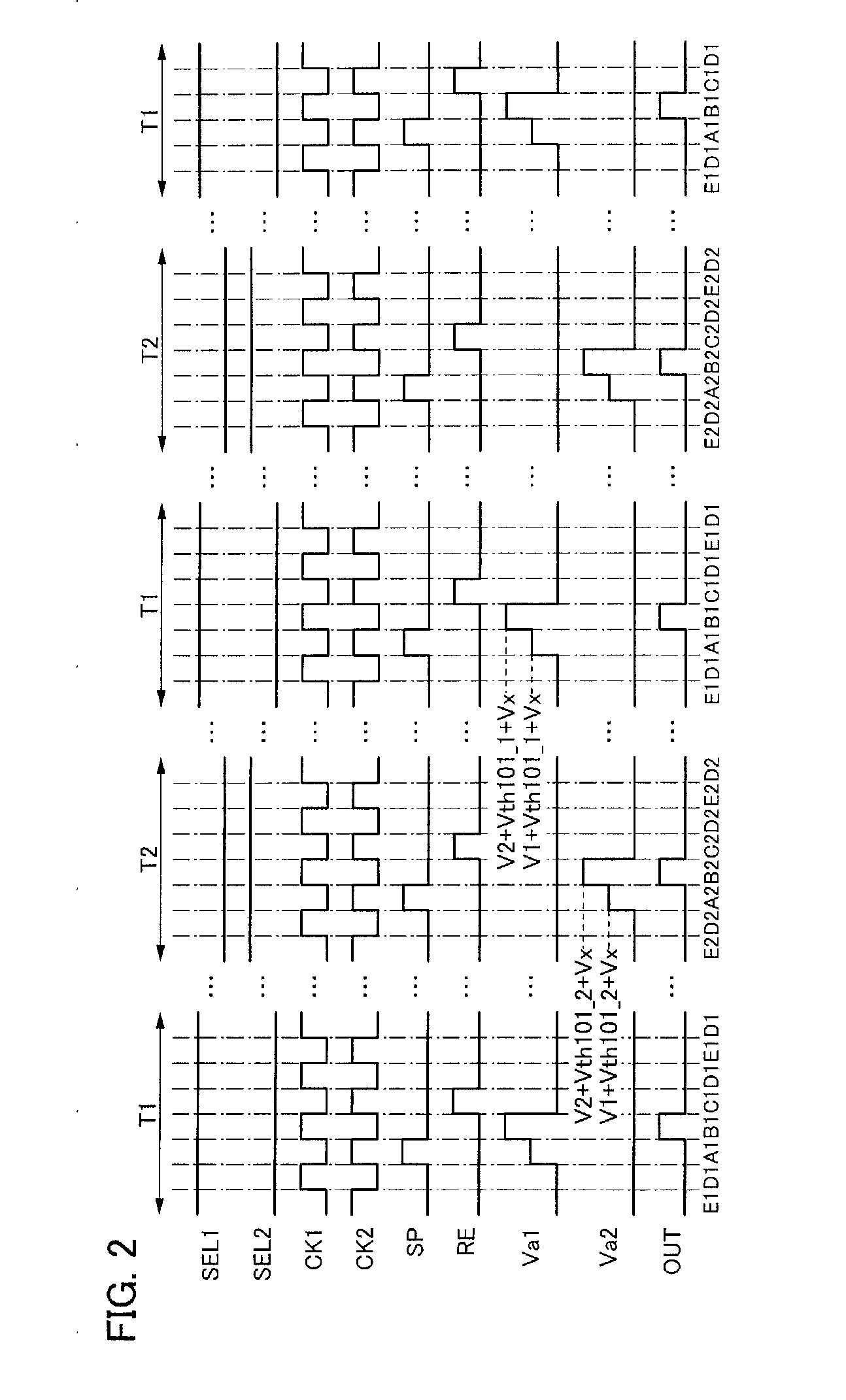
[0119]An example of this embodiment includes a first transistor, a second transistor, and a first circuit. A first terminal of the first transistor is electrically connected to a first wiring and a second terminal of the first transistor is electrically connected to a second wiring. A first terminal of the second transistor is electrically connected to the first wiring and a second terminal of the second transistor is electrically connected to the second wiring. The first circuit is electrically connected to a gate of the first transistor and a gate of the second transistor. The first circuit has the function of raising the gate voltage of the first transistor when a first signal is in a second voltage state and a second signal is in a first voltage state and the function of raising the gate voltage of the second transistor when the first signal is in the second voltage state and a third signal is in the first voltage state.

[0120]An example of a semiconductor device in this embodime...

embodiment 2

[0216]An example of this embodiment includes a first transistor, a second transistor, a first circuit, a second circuit, and a third circuit. A first terminal of the first transistor is electrically connected to a first wiring and a second terminal of the first transistor is electrically connected to a second wiring. A first terminal of the second transistor is electrically connected to the first wiring and a second terminal of the second transistor is electrically connected to the second wiring. The first circuit is electrically connected to a gate of the first transistor and a gate of the second transistor. The second circuit is electrically connected to the gate of the first transistor, the gate of the second transistor, and the second wiring. The third circuit is electrically connected to the gate of the first transistor, the gate of the second transistor, and the second wiring. The first circuit has the function of raising the gate voltage of the first transistor when a first s...

embodiment 3

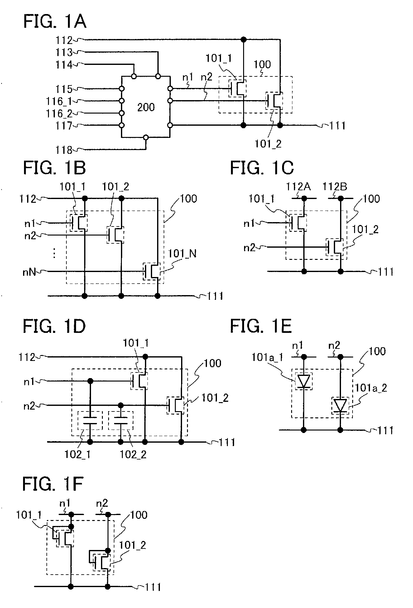
[0287]In this embodiment, an example of a semiconductor device will be described. The semiconductor device in this embodiment can be used for the circuit 400 described in Embodiment 2. Note that description of the content described in Embodiments 1 and 2 is not repeated. Note that the content described in this embodiment can be combined with the content described in Embodiments 1 and 2, as appropriate.

[0288]First, an example of the circuit 400 will be described with reference to FIG. 21A. In the example of FIG. 21A, the circuit 400 includes a circuit 600, a plurality of transistors, that is, transistors 401_1 and 401_2, and a transistor 402. The transistors 401_1 and 401_2 and the transistor 402 preferably have the same polarity as the transistors 101_1_1 and 101_2, which are n-channel transistors. Note that this embodiment is not limited to this, that is, the transistors 401_1 and 401_2 and the transistor 402 can be p-channel transistors. Note that the circuit 400 need not have all...


PUM


Abstract

A driver circuit includes a circuit 200, a transistor 1011, and a transistor 1012. A signal is selectively input from the circuit 200 to a gate of the transistor 1011 and the transistor 1012, so that the transistor 1011 and the transistor 1012 are controlled to be on or off. The transistor 1011 and the transistor 1012 are turned on or off; thus, the wiring 112 and the wiring 111 become conducting or non-conducting.

Description

BACKGROUND OF THE INVENTION[0001]1. Field of the Invention[0002]The present invention relates to a semiconductor device, a display device, a liquid crystal display device, a light-emitting device, a method for driving these devices, and a method for manufacturing these devices. The present invention particularly relates to a semiconductor device, a display device, a liquid crystal display device, a light-emitting device which include driver circuits formed over the same substrates as pixel portions, and a method for driving these devices. Alternatively, the present invention relates to an electronic device including the semiconductor device, the display device, the liquid crystal display device, or the light-emitting device.[0003]2. Description of the Related Art[0004]In recent years, with the increase of large display devices such as liquid crystal televisions, display devices have been actively developed. In particular, a technique for forming a driver circuit such as a gate drive...

Claims


Application Information

Patent Timeline
Patent Type & Authority Applications(United States)
IPC IPC(8): G09G3/36G09G5/00
CPCG09G3/20G09G3/3688G09G2300/0426G09G2300/0842G09G2310/0267H01L27/124G09G2310/0286G09G2310/0291G02F1/13624G02F1/1368H01L27/1225G09G2310/0275G09G3/3674G09G3/3677G09G2300/0809H01L29/24H01L29/7869G02F2202/10G09G3/3696G09G2330/021
Inventor KIMURA, HAJIMEUMEZAKI, ATSUSHI
Owner SEMICON ENERGY LAB CO LTD
Why Eureka
Try Eureka