Display apparatus, driving method for display apparatus and electronic apparatus

a technology of display apparatus and driving method, applied in the direction of instruments, static indicating devices, etc., can solve problems such as the refinement of pixel size, and achieve the effect of higher definition of display apparatus

Active Publication Date: 2009-04-30
JOLED INC
View PDF4 Cites 15 Cited by
  • Summary
  • Abstract
  • Description
  • Claims
  • Application Information

AI Technical Summary

Benefits of technology

[0015]In the configuration of Patent Document 1, each pixel circuit is provided with a compensation function for the characteristic variation of the organic EL element and a correction function for correction against the variation of the threshold voltage Vth and the mobility μ of the driving transistor as described above. Therefore, even if the I-V characteristic of the organic EL element suffers from long-term deterioration or the threshold voltage Vth or the mobility μ of the driving transistor suffers from secular change, the emission light luminance of the organic EL element can be kept fixed without being influenced by such long-term deterioration or secular change as described above. However, the number of pixels which form the pixel circuit is comparatively great, and this makes an obstacle to refinement of the pixel size and hence to achievement of higher definition of the display apparatus.

Problems solved by technology

However, the number of pixels which form the pixel circuit is comparatively great, and this makes an obstacle to refinement of the pixel size and hence to achievement of higher definition of the display apparatus.

Method used


Image

  • Display apparatus, driving method for display apparatus and electronic apparatus
  • Display apparatus, driving method for display apparatus and electronic apparatus
  • Display apparatus, driving method for display apparatus and electronic apparatus

Examples


Embodiment Construction

System Configuration

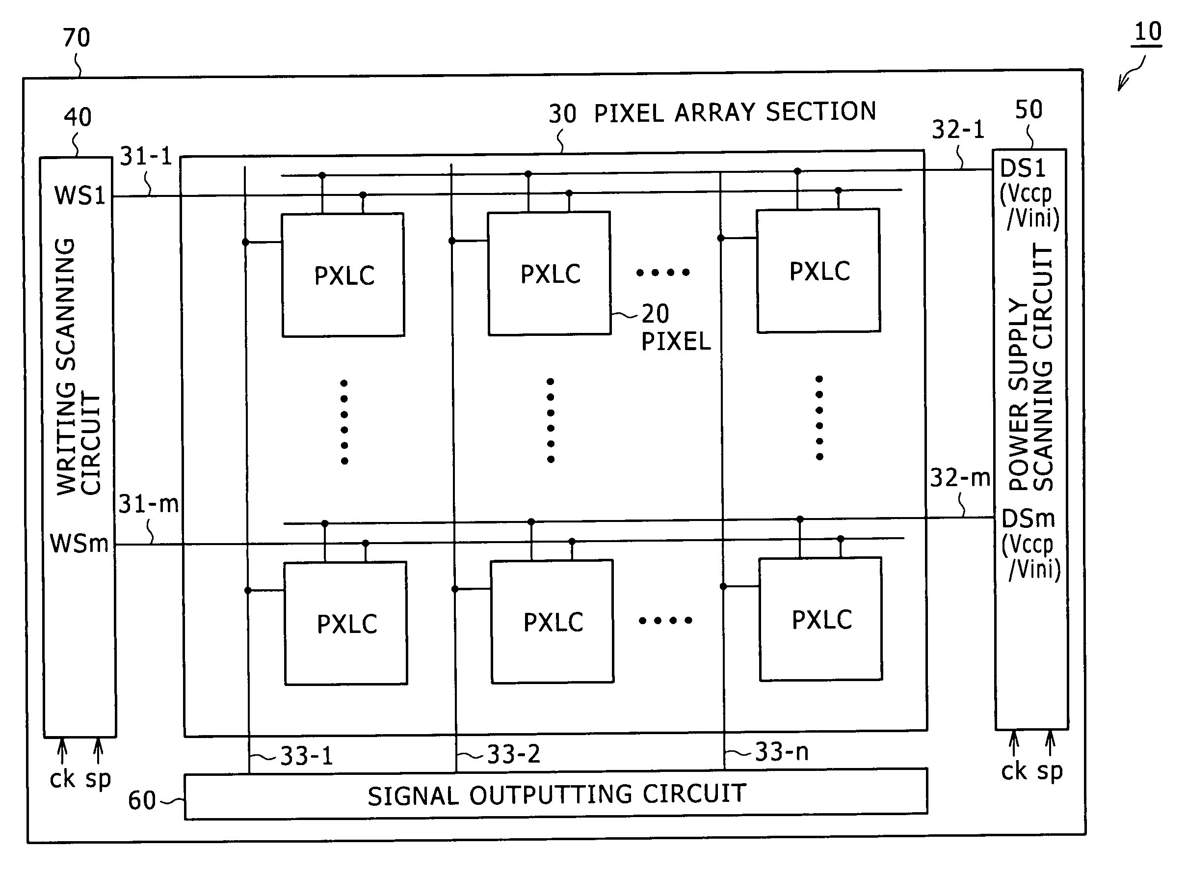
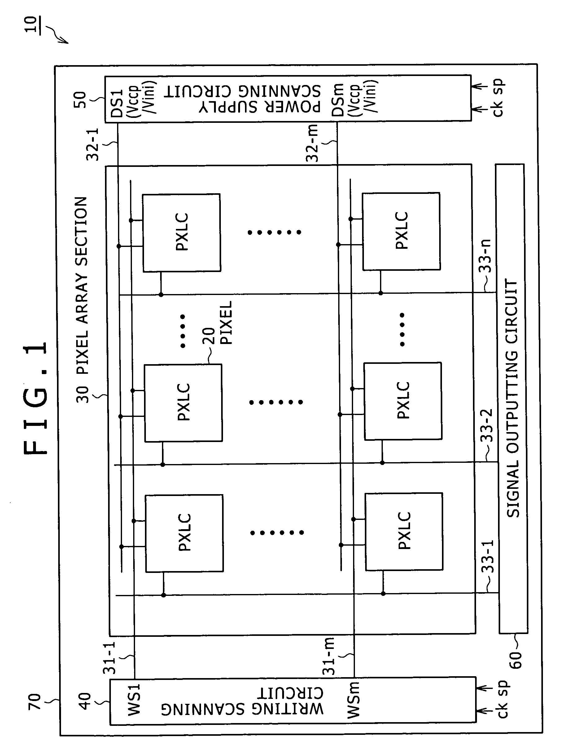
[0045]FIG. 1 shows a general configuration of an active matrix type display apparatus to which an embodiment of the present invention is applied.

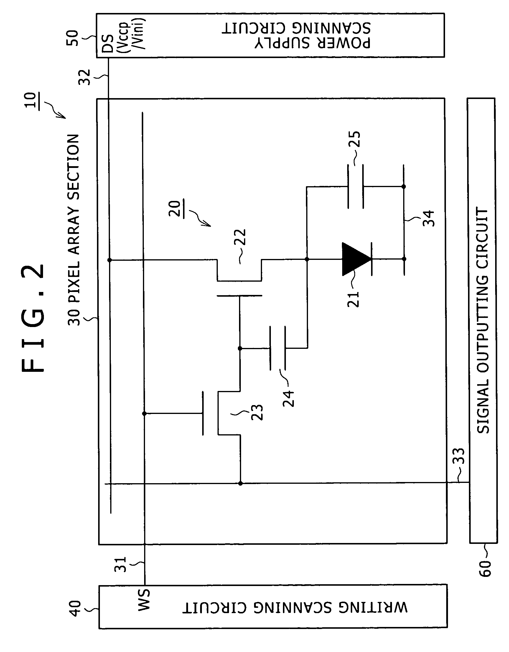
[0046]Here, the active matrix type display apparatus uses, as a light emitting element for a pixel or pixel circuit, an electro-optical element of the current driven type whose emission light luminance varies in response to the value of current flowing therethrough. Thus, it is assumed that the active matrix type display apparatus described below is an active matrix type organic EL display apparatus which uses an organic EL element, that is, an organic electroluminescence element as a light emitting element of a pixel or pixel circuit.

[0047]Referring to FIG. 1, the organic EL display apparatus 10 includes a plurality of pixels (PXLC) 20 including light emitting elements, a pixel array section 30 wherein the pixels 20 are disposed two-dimensionally in rows and columns, that is, in a matrix, and driving sections disposed a...


PUM


Abstract

Disclosed herein is a display apparatus, including: a pixel array section having a plurality of pixels each including an electro-optical element, a writing transistor, a driving transistor, and a holding capacitor; a power supply scanning circuit; and a signal outputting circuit; wherein the power supply scanning circuit is operable to supply a second power supply potential to initialize the potential of a second electrode of the driving transistor and then change over the potential of a power supply line to a first power supply potential; and the signal outputting circuit is operable to output, when the writing transistor is in a conducting state, a first reference potential, supply, midway while a threshold value correction process is carried out, a second reference potential, output a third reference potential within a period within which the writing transistor remains in the conducting state, and output a image signal after the threshold correction process ends.

Description

CROSS REFERENCES TO RELATED APPLICATIONS[0001]The present invention contains subject matter related to Japanese Patent Application JP 2007-277158 filed in the Japan Patent Office on Oct. 25, 2007, the entire contents of which being incorporated herein by reference.BACKGROUND OF THE INVENTION[0002]1. Field of the Invention[0003]This invention relates to display apparatuses, driving methods for a display apparatus and electronic apparatuses, and more particularly to a display apparatus of the flat type or flat panel type wherein a plurality of pixels including electro-optical elements are disposed in rows and columns, that is, in a matrix, and a driving method for the display apparatus and an electronic apparatus including the display apparatus.[0004]2. Description of the Related Art[0005]In recent years, in the field of display apparatus for displaying an image, flat type display apparatus wherein pixels or pixel circuits including light emitting elements are disposed in a matrix hav...

Claims


Application Information

Patent Timeline
Patent Type & Authority Applications(United States)
IPC IPC(8): G09G3/30
CPCG09G3/3233G09G3/3291G09G2300/0819G09G2320/043G09G2300/0866G09G2310/0297G09G2300/0842
Inventor MINAMI, TETSUOTOMIDA, MASATSUGU
Owner JOLED INC
Why Eureka
Try Eureka