Semiconductor device and method for manufacturing the same

a technology of semiconductors and semiconductors, applied in the direction of semiconductor devices, electrical appliances, transistors, etc., can solve the problems of inability to improve the aperture ratio and its reliability, and achieve the effects of high aperture ratio, easy breakage, and high definition of display images

Active Publication Date: 2011-01-13
SEMICON ENERGY LAB CO LTD
View PDF48 Cites 112 Cited by
  • Summary
  • Abstract
  • Description
  • Claims
  • Application Information

AI Technical Summary

Benefits of technology

[0055]Since a thin film transistor is easily broken due to static electricity or the like, a protective circuit for protecting the thin film transistor in the pixel portion is preferably provided over the same substrate for a gate line or a source line. The protective circuit is preferably formed with a non-linear element including an oxide semiconductor.
[0056]In a pixel portion of a display device, by using a film having a light transmitting property for components of a thin film transistor, a high aperture ratio can be achieved even when the size of a pixel is miniaturized for an increase in the number of scan lines, for example, so as to realize high definition of a display image. Further, by using a film having a light transmitting property for components of a thin film transistor, a high aperture ratio can be achieved even when one pixel is divided into a plurality of sub-pixels in order to realize a wide viewing angle.

Problems solved by technology

However, since a conductive film having a light transmitting property is used just for an electrode material in a conventional display panel which uses an oxide semiconductor, an aperture ratio cannot be improved.
In addition, when a display device is manufactured using metal oxide, its reliability has not been taken into consideration.

Method used


Image

  • Semiconductor device and method for manufacturing the same
  • Semiconductor device and method for manufacturing the same
  • Semiconductor device and method for manufacturing the same

Examples


embodiment 1

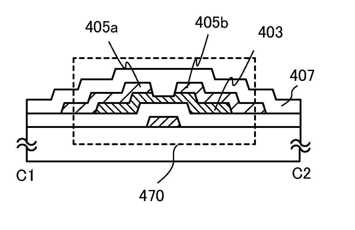
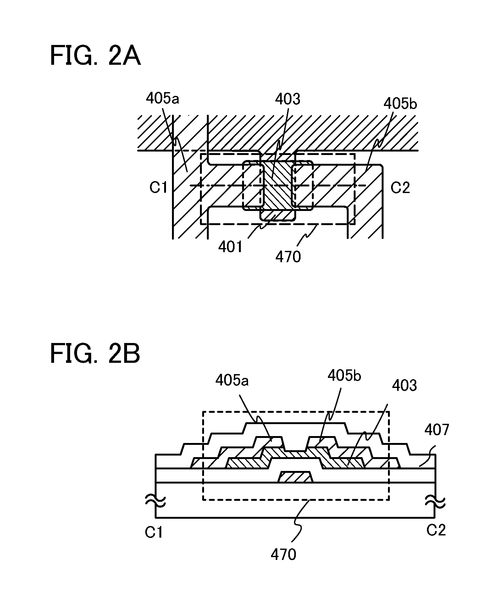
[0079]A semiconductor device and a method for manufacturing a semiconductor device will be described with reference to FIGS. 1A to 1C and FIGS. 2A and 2B. In FIG. 2B, a thin film transistor 470 which is one type of a structure called a channel-etch type is illustrated.

[0080]FIG. 2A is a plan view of the thin film transistor 470 included in a semiconductor device, and FIG. 2B is a cross-sectional view taken along line C1-C2 of FIG. 2A. The thin film transistor 470 is a bottom gate thin film transistor and includes, over a substrate 400 having an insulating surface, a gate electrode layer 401, a gate insulating layer 402, an oxide semiconductor layer 403, a source electrode layer 405a, and a drain electrode layer 405b. In addition, an oxide insulating film 407 is provided to cover the thin film transistor 470 and be in contact with the oxide semiconductor layer 403.

[0081]The substrate 400 having an insulating surface, the gate electrode layer 401, the gate insulating layer 402, the ox...

embodiment 2

[0112]A semiconductor device and a method for manufacturing a semiconductor device which are different from Embodiment 1 will be described with reference to FIGS. 3A to 3D. The portion that is identical to or has a function similar to those described in Embodiment 1 can be formed in a manner similar to that described in Embodiment 1; therefore, repetitive description is omitted.

[0113]FIGS. 3A to 3D are cross-sectional views illustrating a manufacturing process of a thin film transistor 480. The structure of the thin film transistor 480 which is illustrated in FIG. 3D is called an inverted coplanar type (also called a bottom-contact type).

[0114]Similarly to Embodiment 1, the gate electrode layer 401 is provided over the substrate 400 having an insulating surface. An insulating film serving as a base film may be provided between the substrate 400 and the gate electrode layer 401.

[0115]Next, similarly to Embodiment 1, the gate insulating layer 402 is formed over the gate electrode laye...

embodiment 3

[0132]A semiconductor device and a method for manufacturing a semiconductor device which are different from Embodiments 1 and 2 will be described with reference to FIGS. 4A to 4C. The portion that is identical to or has a function similar to those described in Embodiments 1 and 2 can be formed in a manner similar to that described in Embodiments 1 and 2; therefore, repetitive description is omitted.

[0133]FIGS. 4A to 4C are cross-sectional views illustrating a manufacturing process of a thin film transistor 440. The structure of the thin film transistor 440 which is illustrated in FIG. 4C is called a channel stop type.

[0134]Similarly to Embodiment 1, the gate electrode layer 401 is provided over the substrate 400 having an insulating surface. An insulating film serving as a base film may be provided between the substrate 400 and the gate electrode layer 401.

[0135]Next, similarly to Embodiment 1, the gate insulating layer 402 is formed over the gate electrode layer 401. Then, an oxide...


PUM

PropertyMeasurementUnit
temperatureaaaaaaaaaa

Abstract

It is an object to manufacture and provide a highly reliable display device including a thin film transistor with a high aperture ratio which has stable electric characteristics. In a manufacturing method of a semiconductor device having a thin film transistor in which a semiconductor layer including a channel formation region is formed using an oxide semiconductor film, a heat treatment for reducing moisture and the like which are impurities and for improving the purity of the oxide semiconductor film (a heat treatment for dehydration or dehydrogenation) is performed. Further, an aperture ratio is improved by forming a gate electrode layer, a source electrode layer, and a drain electrode layer using conductive films having light transmitting properties.

Description

TECHNICAL FIELD[0001]The present invention relates to a semiconductor device having a circuit formed using a thin film transistor (hereinafter referred to as TFT) and a manufacturing method thereof. For example, the present invention relates to electro-optical devices typified by liquid crystal display panels, or electronic devices which have light-emitting display devices containing an organic light-emitting element as a component.[0002]Note that in this specification, a semiconductor device refers to all devices that can function by utilizing semiconductor characteristics. An electro-optical device, a semiconductor circuit, and an electronic appliance are all semiconductor devices.BACKGROUND ART[0003]Note that as a method for providing a metal auxiliary wiring for a transparent electrode of an electro-optical element, a method by which the metal auxiliary wiring is provided so as to overlap with an upper surface of the transparent electrode or a lower surface of the transparent el...

Claims


Application Information

Patent Timeline
Patent Type & Authority Applications(United States)
IPC IPC(8): H01L29/786H01L21/34
CPCH01L21/02554H01L21/02565H01L27/1225H01L29/7869H01L27/124H01L29/66969H01L2924/0002H01L33/42H01L2924/00H01L29/78618H01L29/78645H01L29/78696H01L27/1255H01L27/1248
Inventor YAMAZAKI, SHUNPEISAKAKURA, MASAYUKI
Owner SEMICON ENERGY LAB CO LTD
Why Eureka
Try Eureka