Electronic component manufacturing apparatus and electronic component manufacturing method

a manufacturing apparatus and electronic component technology, applied in the direction of capacitor manufacturing, variable capacitors, fixed capacitor details, etc., can solve the problems of difficult in practice to check whether such small electronic component chips have been properly turned, and become difficult to accurately turn electronic component chips, so as to achieve the effect of reliable turning of electronic component chips

Active Publication Date: 2014-12-25
MURATA MFG CO LTD
View PDF2 Cites 0 Cited by
  • Summary
  • Abstract
  • Description
  • Claims
  • Application Information

AI Technical Summary

Benefits of technology

[0013]In view of the current circumstances of the related art described above, an object of the present invention is to provide an electronic component manufacturing apparatus and an electronic component manufacturing method using the electronic component manufacturing apparatus in which it is possible to reliably turn electronic component chips even if they are small in size.
[0019]In the electronic component manufacturing apparatus and the electronic component manufacturing method according to the preferred embodiments of the present invention, in a state where at least one electronic component chip having a pair of opposite surfaces is held between the first and second plates, with one surface adhering to the adhesive surface of the first plate and the other surface being in contact with the second plate, at least one of the first and second plates can be moved in accordance with the turning path of the electronic component chip. It is thus possible to turn the electronic component chip. That is, since it is possible to reliably turn the electronic component chip along its turning path, the electronic component chip can be properly turned even if the electronic component chip is small in size or even if the elastic layers are deformed by being pressed into contact therewith by the electronic component chip.
[0020]The electronic component manufacturing apparatus and the electronic component manufacturing method according to the preferred embodiments of the present invention are suitable for use in the process of applying paste to opposite end faces of electronic component chips, and make it possible to reliably apply paste to both end faces of the electronic component chips.

Problems solved by technology

However, Japanese Unexamined Patent Application Publication No. 2010-141145 does not describe in detail any specific method or apparatus for turning the electronic component chip.
In this technique, as the size of the electronic component chips decreases, it becomes difficult to accurately turn the electronic component chips due to, for example, deformation of the elastic member.
Moreover, it is difficult in practice to check whether such small electronic component chips have been properly turned, because of a small distance between elastic members on both sides of the electronic component chips.

Method used


Image

  • Electronic component manufacturing apparatus and electronic component manufacturing method
  • Electronic component manufacturing apparatus and electronic component manufacturing method
  • Electronic component manufacturing apparatus and electronic component manufacturing method

Examples


Embodiment Construction

[0033]The present invention will be clarified by describing specific preferred embodiments of the present invention with reference to the drawings.

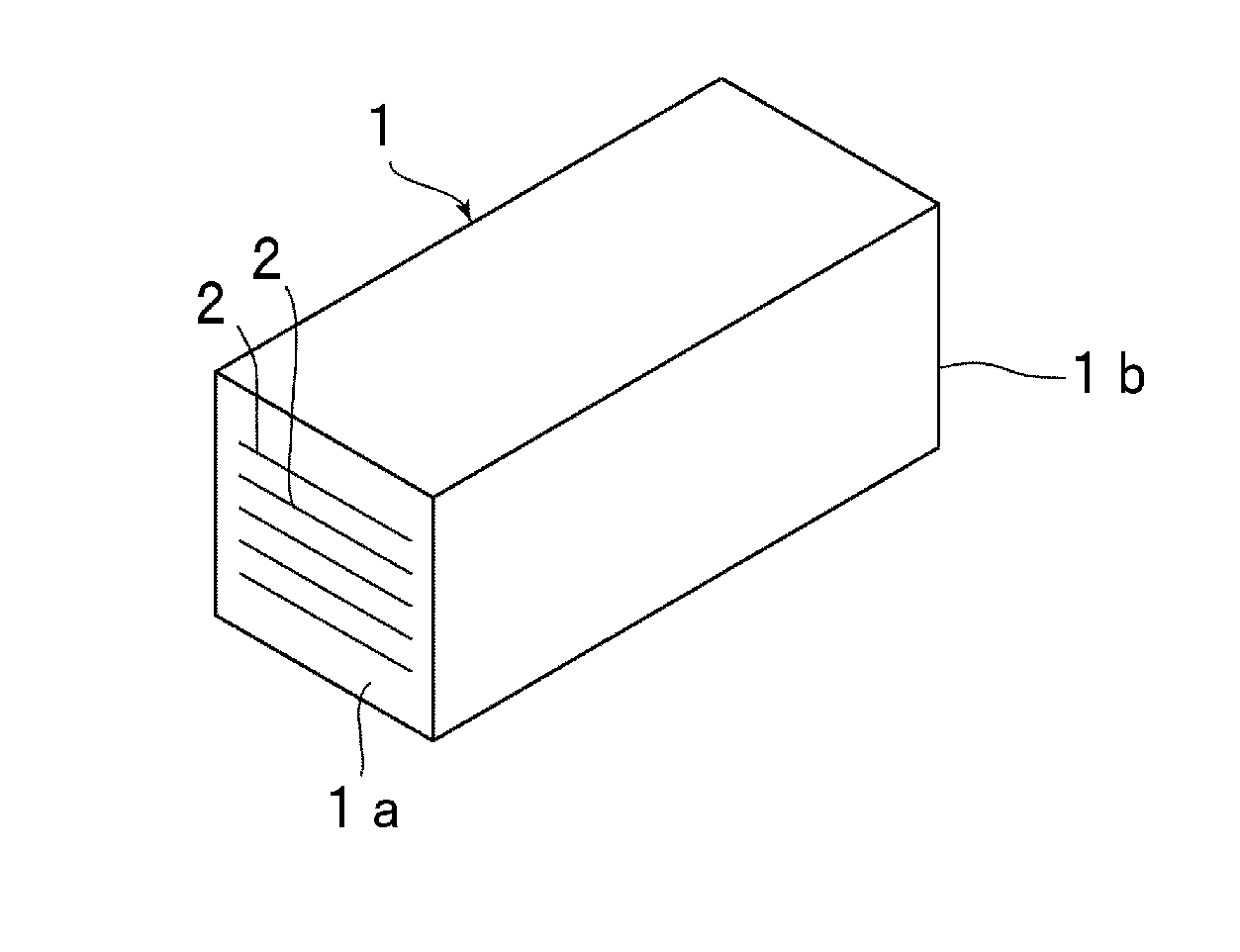
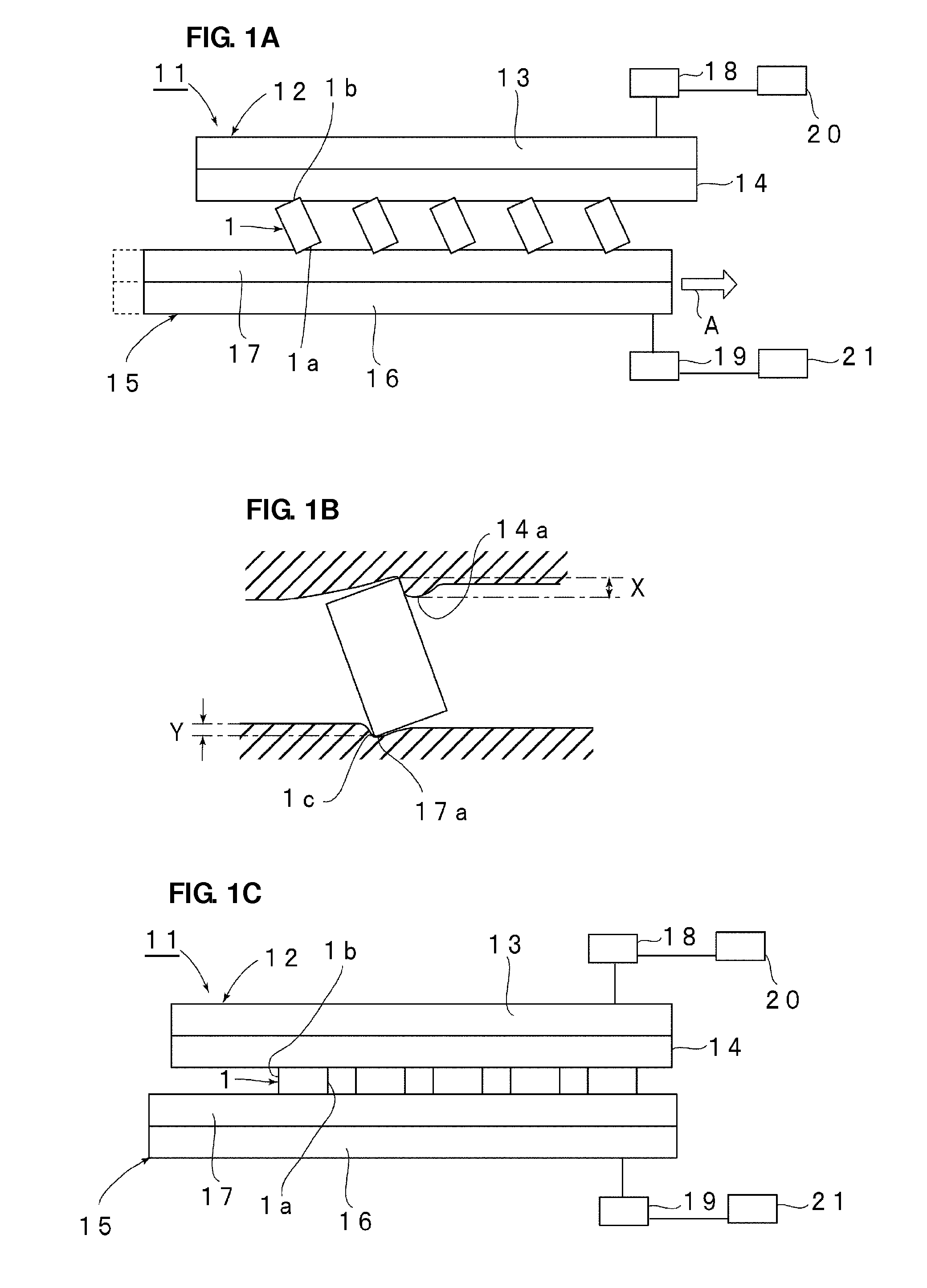
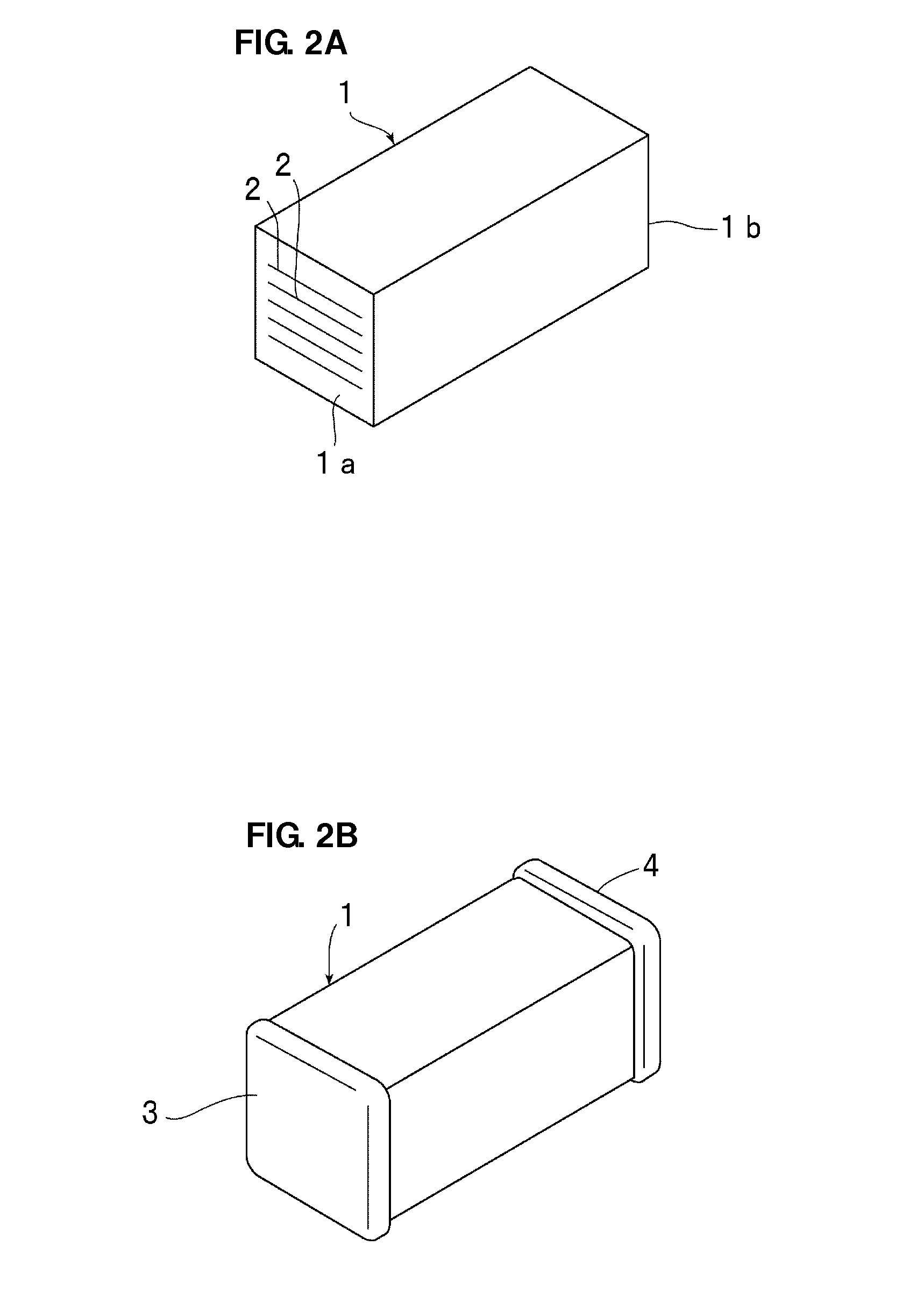
[0034]In an electronic component manufacturing method of the present preferred embodiment, conductive pastes are applied to and baked on both end faces of an electronic component chip 1 illustrated in FIG. 2A. The electronic component chip 1 is a ceramic sintered body having a plurality of internal electrodes 2. In the ceramic sintered body, the internal electrodes 2 illustrated in FIG. 2A and a plurality of other internal electrodes are alternately stacked, with ceramic layers interposed between adjacent internal electrodes. The plurality of internal electrodes 2 are exposed to an end face 1a of the electronic component chip 1. The plurality of other internal electrodes alternately stacked with the plurality of internal electrodes 2, as described above, are exposed to an end face 1b of the electronic component chip 1. The end face 1a and...


PUM

PropertyMeasurementUnit
angleaaaaaaaaaa
angleaaaaaaaaaa
distanceaaaaaaaaaa

Abstract

An electronic component manufacturing method includes the steps of preparing at least one electronic component chip having a first surface and a second surface opposite each other; holding the electronic component chip between a first plate and a second plate such that the first surface is in contact with a first elastic layer of the first plate and the second surface is in contact with a second elastic layer of the second plate; and turning the electronic component chip by relatively moving the first and second plates in a planar direction thereof using a planar movement mechanism and moving the first and second plates in accordance with a turning path of the electronic component chip using the planar movement mechanism and a vertical movement mechanism.

Description

BACKGROUND OF THE INVENTION[0001]1. Field of the Invention[0002]The present invention relates to electronic component manufacturing apparatuses and electronic component manufacturing methods used, for example, to apply conductive paste to a plurality of end faces of electronic component chips. In particular, the present invention relates to an electronic component manufacturing apparatus in which electronic component chips are held between a pair of opposite plates and turned by relatively moving the pair of plates, and also relates to an electronic component manufacturing method using the electronic component manufacturing apparatus.[0003]2. Description of the Related Art[0004]In an electronic component, such as a monolithic capacitor, electrodes are formed on a plurality of surfaces of an electronic component chip. As examples of electrode forming methods, methods for applying and baking conductive paste have been widely used. For efficient application of conductive paste, a varie...

Claims


Application Information

Patent Timeline
Patent Type & Authority Applications(United States)
IPC IPC(8): H01G13/00
CPCH01G13/00H01G4/232H01G4/30H01G13/006Y10T29/43Y10T29/5313Y10T29/53174Y10T29/53178H01G4/12
Inventor OGATA, KATSUNORIMIZUKAMI, MIYUKI
Owner MURATA MFG CO LTD
Why Eureka
Try Eureka