Switching power supply apparatus

a power supply and power supply technology, applied in the direction of electric variable regulation, process and machine control, instruments, etc., can solve the problems of drop in power conversion efficiency, etc., to prevent the drop in conversion efficiency, increase the invalid time of power conversion, and zero voltage switching of the switching element

Active Publication Date: 2014-12-25
FUJI ELECTRIC CO LTD
View PDF5 Cites 19 Cited by
  • Summary
  • Abstract
  • Description
  • Claims
  • Application Information

AI Technical Summary

Benefits of technology

[0033]As a consequence, zero voltage switching of the switching element can be easily and effectively implemented, and a drop in conversion efficiency can be prevented. Particularly such a problem as extension of the current peak, due to the increase of invalid time of power conversion caused by temperature dependency or age-based deterioration of components o

Problems solved by technology

On the other hand, because of age-based deterioration and the dispersion of component characteristics constituting the switching power supply apparatus, the input voltage Vin may be changed, which may result in a change in the output voltage Vout and a change in the FB voltage.
As a result, an invalid time of power conversion increases, hence the current peak extends and loss in the switching element Q1 or Q2 increases, which results in a drop in power conversion efficiency.
As a result, not only is the zero v

Method used


Image

  • Switching power supply apparatus
  • Switching power supply apparatus
  • Switching power supply apparatus

Examples


embodiment 1

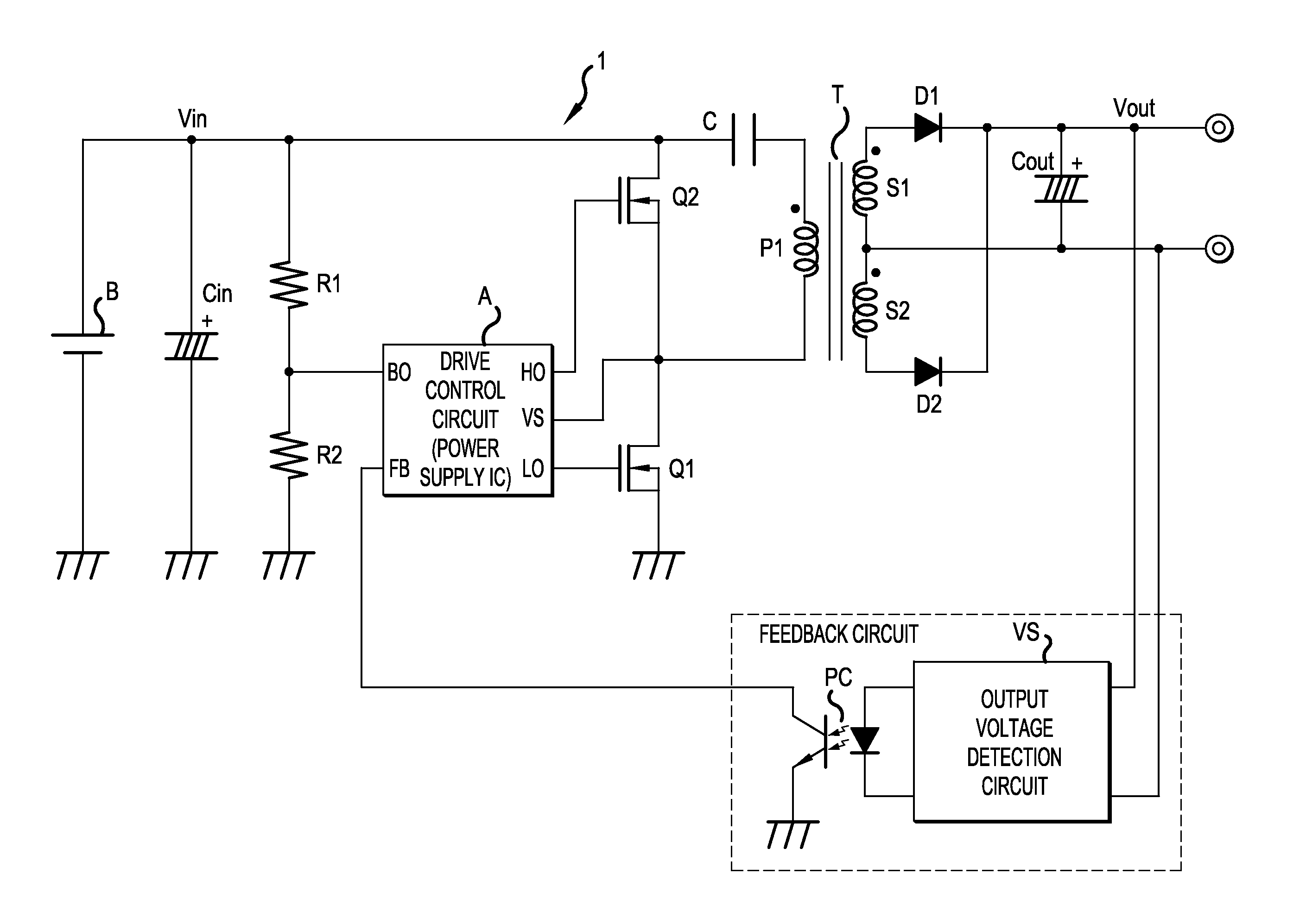
[0053]FIG. 1 is a schematic block diagram of a switching power supply apparatus 1 constructing a resonance type converter of the present invention. In FIG. 1, a composing element the same as the above mentioned conventional switching power supply apparatus 1 shown in FIG. 11 is denoted with a same reference symbol. Redundant description on the configuration of a composing element the same as the conventional apparatus and the functions thereof is therefore omitted.

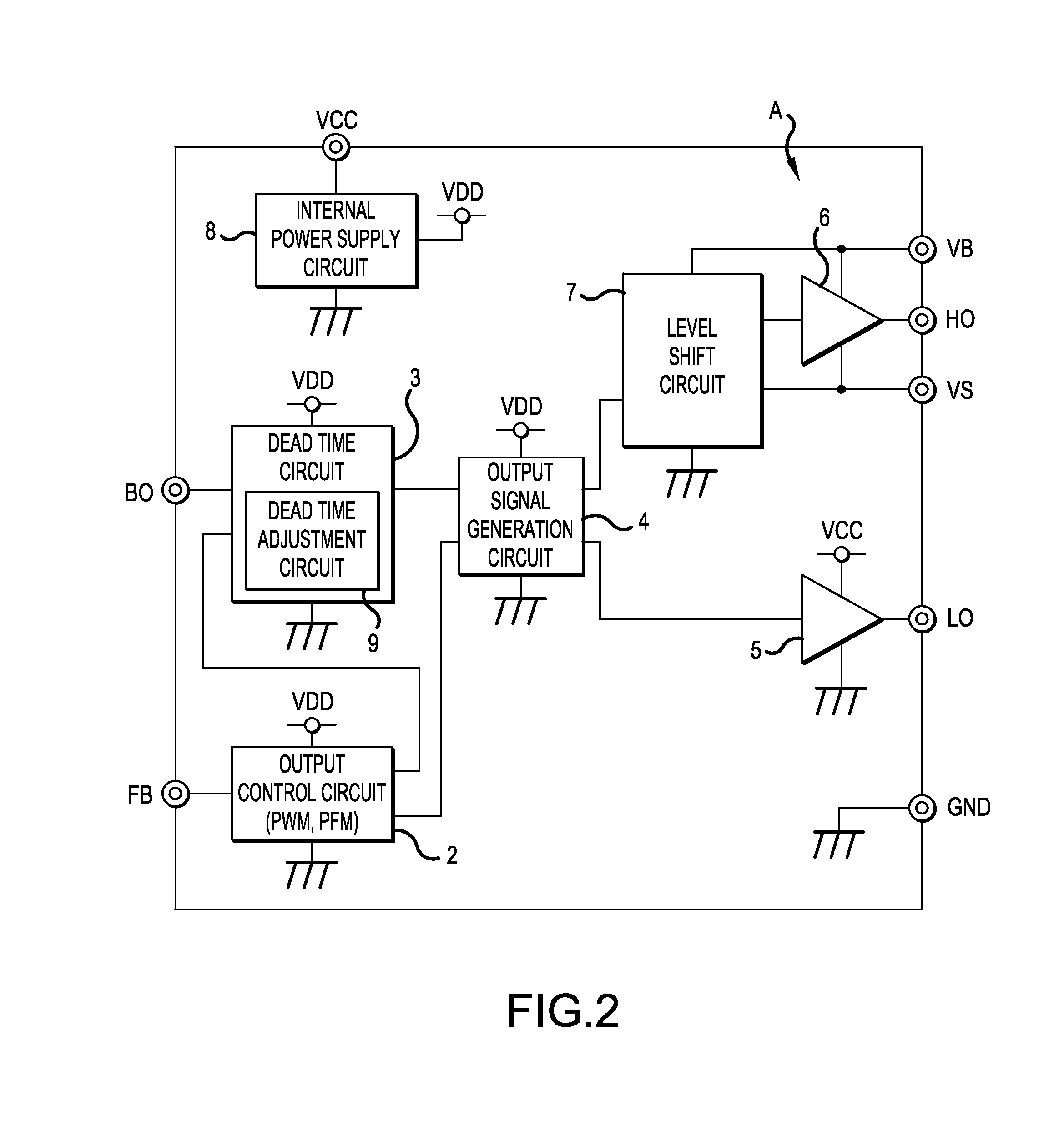
[0054]A characteristic of the switching power supply apparatus 1 according to Embodiment 1 is that input voltage Vin is divided and detected using the voltage dividing resistors R1 and R2, and this detected input voltage Vin is inputted to the drive control circuit A as a BO voltage. Another characteristic is that in the drive control circuit A, the pulse width Tdt of the dead time signal generated by the dead time circuit 3 is adjusted based on the BO voltage.

[0055]In other words, a dead time adjustment circuit 9 is disp...

embodiment 2

[0064]FIG. 6 is a schematic block diagram of a drive control circuit A of a switching power supply apparatus , which is configured to adjust the pulse width Tdt of the dead time signal in accordance with the change of the FB voltage. In the drive control circuit A, a dead time adjustment circuit 9a is disposed as an attachment to the dead time circuit 3. In the dead time adjustment circuit 9a, the pulse width Tdt of the dead time signal generated by the dead time circuit 3 is adjusted in accordance with the change of the FB voltage. In FIG. 6 as well, a same composing element as the above mentioned drive control circuit A shown in FIG. 12 is denoted with a same reference symbol, and redundant description on the same composing element is omitted.

[0065]Specifically, the dead time circuit 3 and the dead time adjustment circuit 9a are configured as shown in FIG. 7, for example. Just like the dead time adjustment circuit 9 shown in FIG. 3, the dead time adjustment circuit 9a includes: a ...

embodiment 3

[0073]FIG. 10 is a schematic block diagram of a switching power supply apparatus of the present invention, and the switching power supply apparatus is constructed by a synchronous rectification boost converter. The synchronous rectification boost converter includes: a first switching element Q1 that is connected to a DC voltage source B via an inductor L, and stores power in the inductor L when the switching element Q1 is turned ON; and a second switching element Q2 that turns ON when the first switching element Q1 is OFF, and transfers the power stored in the inductor L to the output capacitor Cout using resonance of the inductor L, so as to obtain the output voltage Vout.

[0074]The first and second switching elements Q1 and Q2 are alternately turned ON / OFF by the drive control circuit A, just like Embodiments 1 and 2 described above. The synchronous rectification boost converter shown in FIG. 10 is configured such that the output voltage Vout is divided and detected via the voltag...


PUM


Abstract

A switching power supply apparatus includes: a dead time circuit that receives an output control signal and generates dead time signal to specify a time width when both first and second switching elements are turned OFF; an output signal generation circuit that generates first and second output signals which specify the ON time of the first and second switching elements respectively in accordance with the output control signal and the dead time signal; and a dead time adjustment circuit that adjusts the turn ON timings of the first and second switching elements by changing the time width of the dead time signal in accordance with the change of voltage of the DC input power or the change of the output voltage of the capacitor.

Description

CROSS-REFERENCE TO RELATED APPLICATIONS[0001]This application is a continuation of International Application No. PCT / JP2013 / 072477, filed on Aug. 22, 2013, and is based on and claims priority to Japanese Patent Application No. JP 2012-187071, filed on Aug. 27, 2012. The disclosure of the Japanese priority application and the PCT application in their entirety, including the drawings, claims, and the specification thereof, are incorporated herein by reference.BACKGROUND[0002]1. Field of the Invention[0003]Embodiments of the present invention relate to a switching power supply apparatus in which power conversion efficiency has been improved.[0004]2. Discussion of the Background[0005]A resonance type converter is known as a switching power supply apparatus for use in various electronic equipment. The resonance type converter is constructed by connecting a primary winding of an insulation transformer to a DC voltage source via a capacitor. A DC resonance circuit is formed by a leakage in...

Claims


Application Information

Patent Timeline
IPC IPC(8): H02M3/335H02M1/08
CPCH02M3/33523H02M1/08H02M3/33569H02M1/38H02M3/33553Y02B70/10H02M1/0058H02M3/01H02M3/33571
Inventor OHASHI, HIDETOMO
Owner FUJI ELECTRIC CO LTD
Why Eureka
Try Eureka