Circuit module and method of producing the same

a technology of circuit modules and circuits, applied in the direction of electrical apparatus construction details, electrical apparatus casings/cabinets/drawers, semiconductor/solid-state device details, etc., can solve the problems of easy burnt sealing resin, difficult selective removal of only a part of electromagnetic shield film, damage to electronic components located immediately below the removal part, etc., to reduce electrical influence

Inactive Publication Date: 2015-01-15
TAIYO YUDEN KK
View PDF7 Cites 35 Cited by
  • Summary
  • Abstract
  • Description
  • Claims
  • Application Information

AI Technical Summary

Benefits of technology

[0008]In view of the circumstances as described above, it is desirable to provide a circuit module capable of reducing el...

Problems solved by technology

In the configuration described in Japanese Patent Application Laid-open No. 2012-009611, however, it is difficult to selectively remove only a part of the electromagnetic shield film.
For example, in the case where the electromagnetic shield film is intended to be removed by laser irradiation, because an absorption coefficient of a laser beam of an electromagnetic shield film being a conductor is different from that of a sealing resin including an insulating resin, the sealing resin is easily burned off and the electronic component located immediately below the removal part is...

Method used


Image

  • Circuit module and method of producing the same
  • Circuit module and method of producing the same
  • Circuit module and method of producing the same

Examples


first embodiment

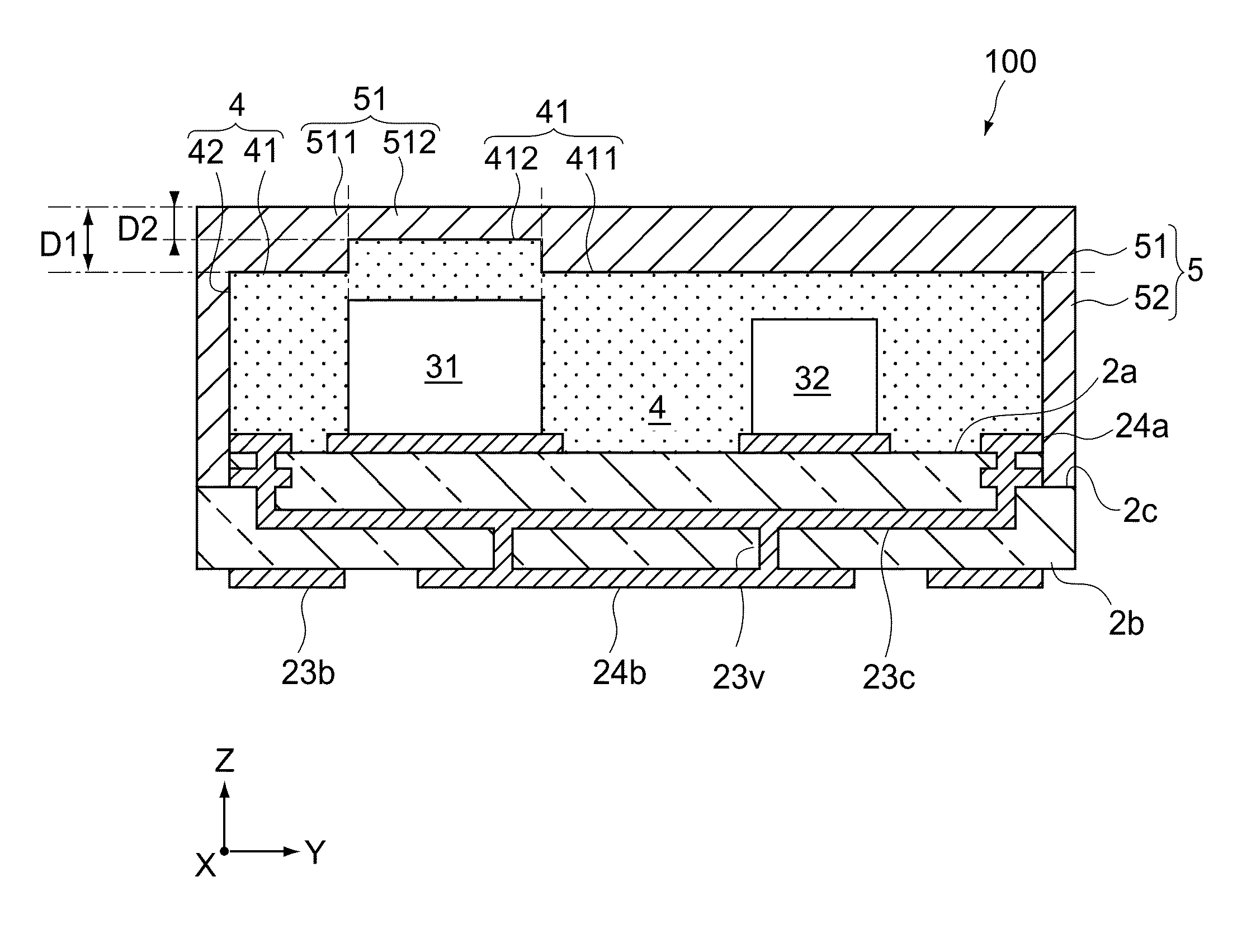
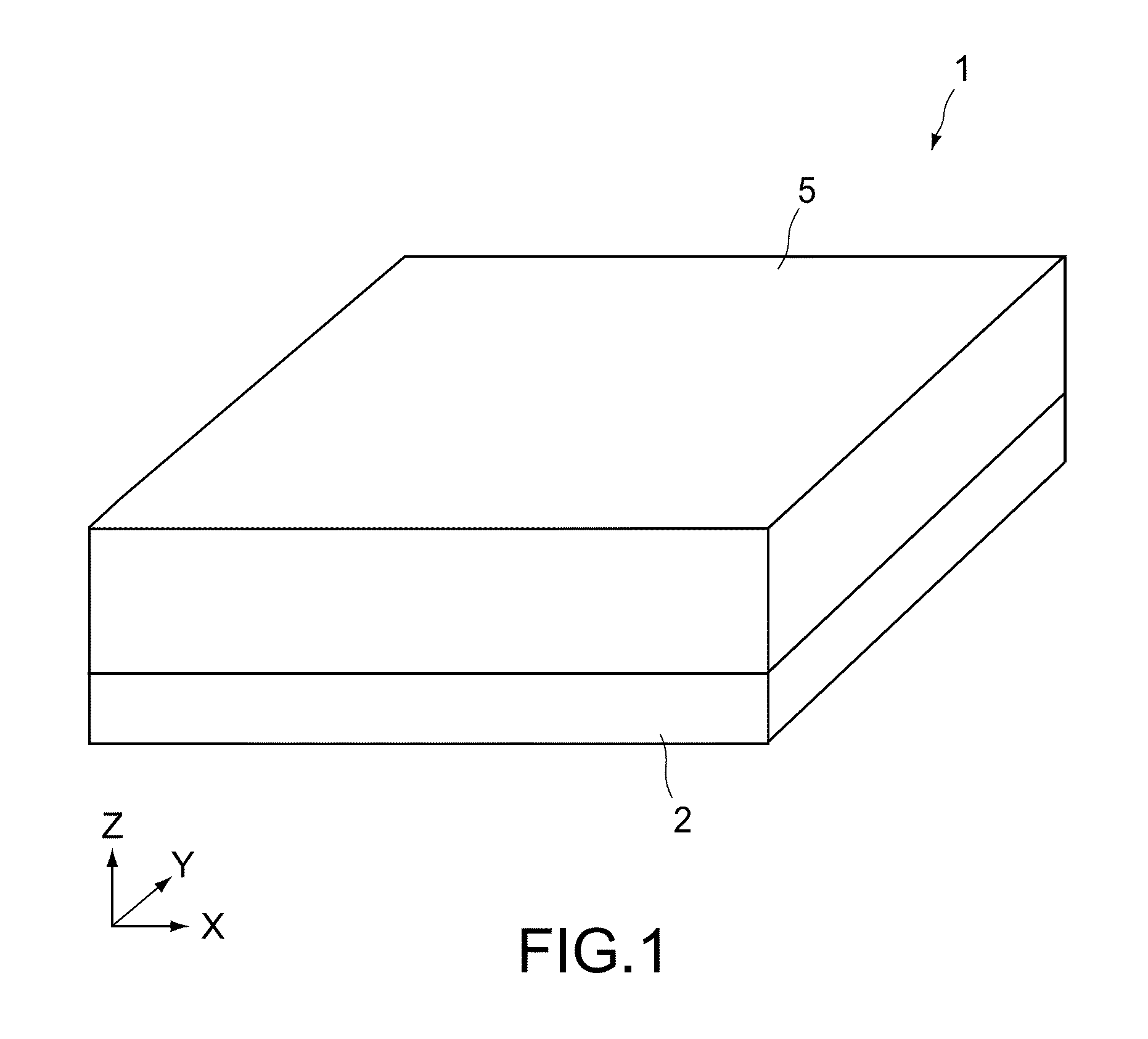
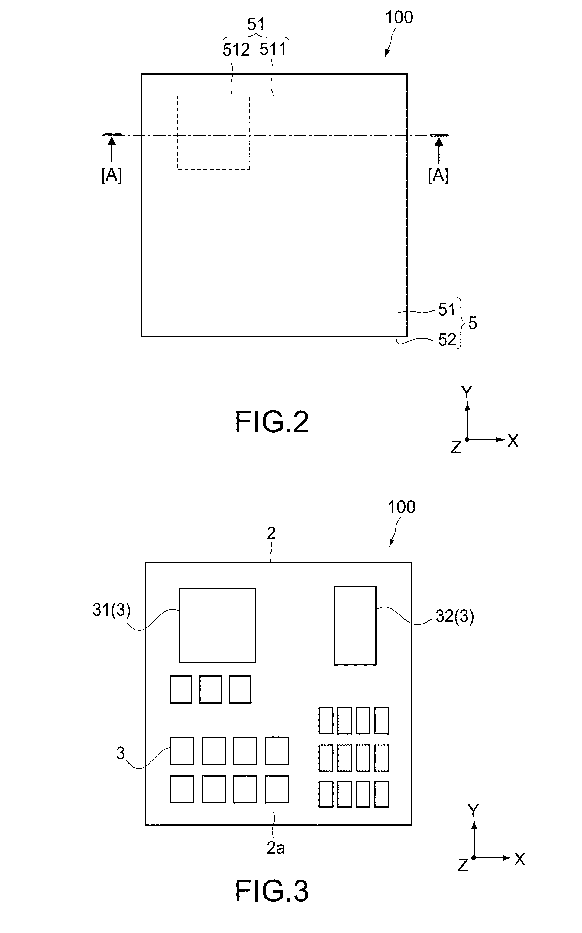
[0058]FIGS. 1 to 4 are each a diagram showing a circuit module according to an embodiment of the present disclosure. FIG. 1 is a perspective view, FIG. 2 is a plan view, FIG. 3 is a plan view of a wiring substrate, and FIG. 4 is a cross-sectional view taken along the direction of the line [A]-[A] of FIG. 2.

[0059]It should be noted that in each figure, X-, Y-, and Z-axes represent triaxial directions orthogonal to each other, and the Z-axis direction corresponds to the thickness direction of the circuit module. It should be noted that the configuration of each portion is exaggeratingly shown in order to facilitate understanding, and the sizes of the members or the ratios of the sizes of the members do not necessarily correspond to each other in the figures.

[0060](Configuration of Circuit Module)

[0061]A circuit module 100 according to this embodiment includes a wiring substrate 2, an electronic component 3, a sealing layer 4, and a conductive shield 5.

[0062]The circuit module 100 is c...

second embodiment

[0120]FIG. 10 is a schematic cross-sectional view showing a circuit module according to a second embodiment of the present disclosure, which corresponds to the cross-sectional view shown in FIG. 4. Hereinafter, the configuration different from that of the first embodiment will be mainly described, and the same configuration as that according to the above-mentioned embodiment will be denoted by the same reference symbols and a description thereof will be omitted or simplified.

[0121]In a circuit module 100B according to this embodiment, a conductive shield 5B covers a second surface 42B of a sealing layer 4B and a first sealing area 411B of a first surface 41B, and does not cover a second sealing area 412B. Specifically, the conductive shield 5B has an opening 513B exposing the second sealing area 412B.

[0122]According to this embodiment, it is also possible to prevent the parasitic capacitance (capacitive coupling) between the electronic component 31 and the conductive shield 5B from ...

third embodiment

[0129]FIG. 11 is a schematic cross-sectional view showing a circuit module according to a third embodiment of the present disclosure, which corresponds to the cross-sectional view shown in FIG. 4. Hereinafter, the configuration different from that of the first embodiment will be mainly described, and the same configuration as that according to the above-mentioned embodiment will be denoted by the same reference symbols and a description thereof will be omitted or simplified.

[0130]In a circuit module 100C according to this embodiment, a conductive shield 5C covers the outer surface of a sealing layer 4C, i.e., a second surface 42C and a first sealing area 411C and second sealing area 412C of a first surface 41C, similar to the first embodiment. However, the circuit module 100C is different from the first embodiment in that a first shield portion 51C is formed with a substantially uniform thickness.

[0131]Specifically, as shown in FIG. 11, the first shield portion 51C of the conductive...


PUM

PropertyMeasurementUnit
Thicknessaaaaaaaaaa
Electrical conductoraaaaaaaaaa
Areaaaaaaaaaaa

Abstract

A circuit module includes a wiring substrate, an electronic component, a sealing layer, and a conductive shield. The wiring substrate has a mount surface. The electronic component is mounted on the mount surface. The sealing layer is formed of an insulating material, covers the electronic component, and has a first surface and a second surface, the first surface being opposite to the mount surface and having a first sealing area and a second sealing area, the second sealing area projecting from the first sealing area to an opposite side of the mount surface, the second surface being connected to the mount surface and the first surface. The conductive shield covers at least the second surface and the first sealing area of the first surface.

Description

CROSS-REFERENCE TO RELATED APPLICATION[0001]This application claims the benefit under 35 U.S.C. §119 of Japanese Patent Application No. 2013-144579, filed Jul. 10, 2013, which is hereby incorporated by reference in its entirety.BACKGROUND OF THE INVENTION[0002]The present disclosure relates to a circuit module having an electromagnetic shielding function and a method of producing the circuit module.[0003]A circuit module that has a substrate on which a plurality of electronic components are mounted and is installed in various electronic apparatuses has been known. In general, such a circuit module employs a configuration that has an electromagnetic shielding function to prevent an electromagnetic wave from leaking to the outside of the module and entering from the outside.[0004]In recent years, electronic components mounted in a circuit module are diversified while the circuit module is expected to be lower in height. For example, in the case where the entire circuit module is to be...

Claims


Application Information

Patent Timeline
IPC IPC(8): H05K9/00H05K3/28H05K5/06H05K3/22
CPCY10T29/49146H05K3/22H05K9/0007H05K5/065H05K3/285H01L21/561H01L21/565H01L21/568H01L23/3121H01L23/3135H01L23/552H01L24/97H01L2224/16225H01L2224/32225H01L2224/48227H01L2224/97H01L2924/12042H01L2924/15192H01L2924/15313H01L2924/181H01L2924/1815H01L2924/19105H05K1/0215H05K1/0216H05K3/284H05K2201/0919H05K2201/0979H05K2201/09845H05K2203/0191H05K2203/085H05K2203/1316H01L2224/85H01L2224/81H01L2924/00H01L2924/00012
Inventor SHIMAMURA, MASAYAMUGIYA, EIJIKITAZAKI, KENZOKAI, TAKEHIKOIMAI, MASAFUMIITO, ATSUSHI
Owner TAIYO YUDEN KK
Why Eureka
Try Eureka