Unlock instant, AI-driven research and patent intelligence for your innovation.

Multi-bit memory device and on-chip buffered program method thereof

Active Publication Date: 2015-02-12
SAMSUNG ELECTRONICS CO LTD
View PDF7 Cites 6 Cited by
  • Summary
  • Abstract
  • Description
  • Claims
  • Application Information

AI Technical Summary

Benefits of technology

The patent describes a method for programming a multi-bit memory device. The method involves storing page data in a buffer and then transferring it to a different buffer for programming in a different region of the memory cell array. The method also includes performing a programming operation on a region based on the previous data stored in a different region. The technical effects of this method include improving programming speed and accuracy in multi-bit memory devices.

Problems solved by technology

Volatile memory devices operate fast but lose stored data when power is not supplied thereto.

Method used


Image

  • Multi-bit memory device and on-chip buffered program method thereof
  • Multi-bit memory device and on-chip buffered program method thereof
  • Multi-bit memory device and on-chip buffered program method thereof

Examples


Embodiment Construction

[0023]Exemplary embodiments of the inventive concept will be described below in detail with reference to the accompanying drawings. However, the inventive concept may be embodied in different forms and should not be construed as limited to the embodiments set forth herein. In the drawings, the thickness of layers and regions may be exaggerated for clarity. It will also be understood that when an element is referred to as being on another element or substrate, it may be directly on the other element or substrate, or intervening layers may also be present. It will also he understood that when an element is referred to as being “coupled to” or “connected to” another element, it may be directly coupled to or connected to the other element, or intervening elements may also be present. Like reference numerals may refer to the like elements throughout the specification and drawings.

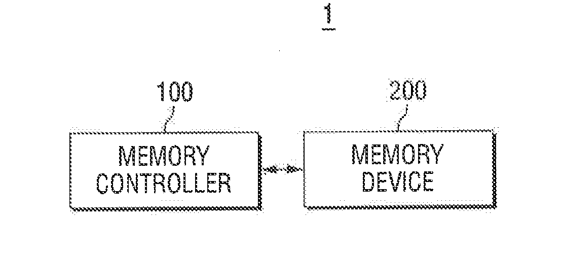
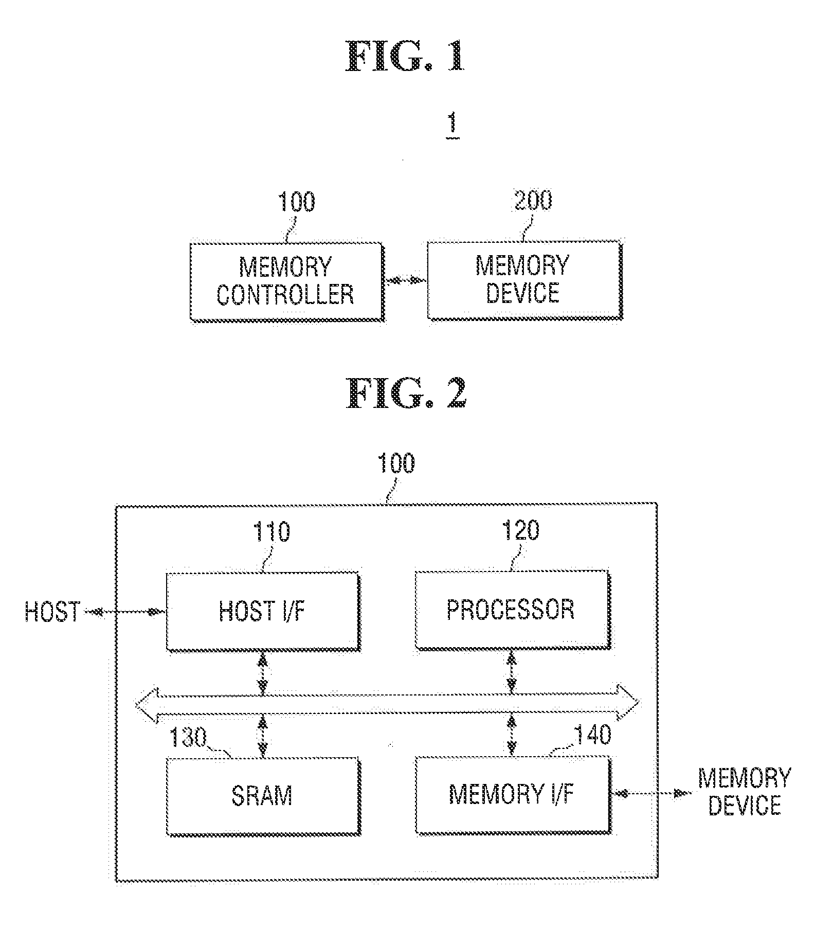
[0024]FIG. 1 is a block diagram of a multi-bit memory system according to an exemplary embodiment of the pres...


PUM


Abstract

A program method of a multi-bit memory device is provided. First page data is programmed in a first region of a memory cell array. The first page data is stored in a first buffer of a page buffer. Second page data is programmed in the first region of the memory cell array. The second page data is stored in a third buffer of the page buffer. Third page data is stored in the first region of the memory cell array. The second page data stored in the third buffer is transferred to a second buffer of the page buffer and the third page data is stored in the third buffer. The first to third page data stored in page buffer are programmed in a second region of the memory cell array.

Description

CROSS-REFERENCE TO RELATED APPLICATION[0001]This application claims priority under 35 U.S.C. §119 to Korean Patent Application No. 10-2013-0094978, filed on Aug. 9, 2013 in the Korean intellectual Property Office, the disclosure of which is incorporated by reference herein in its entirety.TECHNICAL FIELD[0002]The present invention relates to a multi-bit memory device and an on-chip buffered program method thereofDISCUSSION OF RELATED ART[0003]Semiconductor memory devices include volatile memory devices and non-volatile memory devices. Volatile memory devices operate fast but lose stored data when power is not supplied thereto. Non-volatile memory devices retain stored data when power is not supplied thereto. Non-volatile memories include single-bit memory devices whose a unit memory cell stores an 1-bit data and multi-bit memory devices whose a unit memory cell stores multi-level data representing two or more bit data.SUMMARY[0004]According to an exemplary embodiment of the present ...

Claims


Application Information

Patent Timeline
IPC IPC(8): G11C16/10
CPCG11C16/107G11C11/5628G11C16/06G11C16/10G11C16/3418G11C16/04
Inventor CHOI, WAN-SOOKIM, TAEC-JUNNAM, SANG-WOOKLEE, JAE-HWA
Owner SAMSUNG ELECTRONICS CO LTD
Features
  • R&D
  • Intellectual Property
  • Life Sciences
  • Materials
  • Tech Scout
  • Unparalleled Data Quality
  • Higher Quality Content
  • 60% Fewer Hallucinations
Learn More