Non-volatile memory device and self-compensation method thereof

Inactive Publication Date: 2008-07-24
SK HYNIX INC
View PDF3 Cites 50 Cited by
  • Summary
  • Abstract
  • Description
  • Claims
  • Application Information

AI Technical Summary

Benefits of technology

[0016]The present invention relates to a non-volatile memory device and a self-compensation method thereof, in which the thres

Problems solved by technology

The NAND flash memory may have an error due to changed characteristics as it operates for a long time.
If the program and erase operations of the MLC memory device are repeated, electrons are trapped between oxide layers between the floating gate and the substrate of the memory cell, increasing trap charges.
However, as the threshold voltage is shifted lower, the t

Method used


Image

  • Non-volatile memory device and self-compensation method thereof
  • Non-volatile memory device and self-compensation method thereof
  • Non-volatile memory device and self-compensation method thereof

Examples


Embodiment Construction

[0033]Specific embodiments according to the present patent will be described with reference to the accompanying drawings.

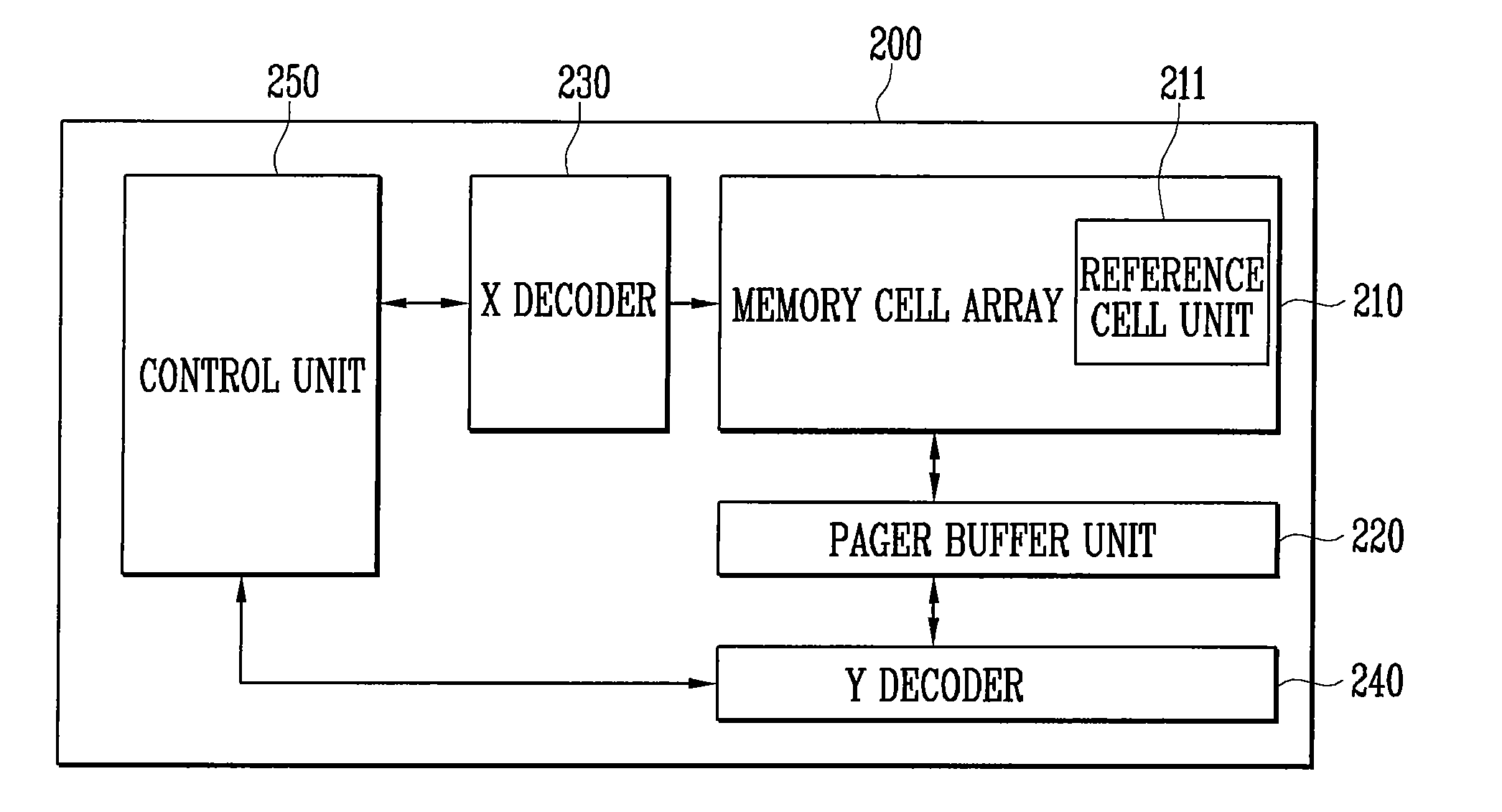
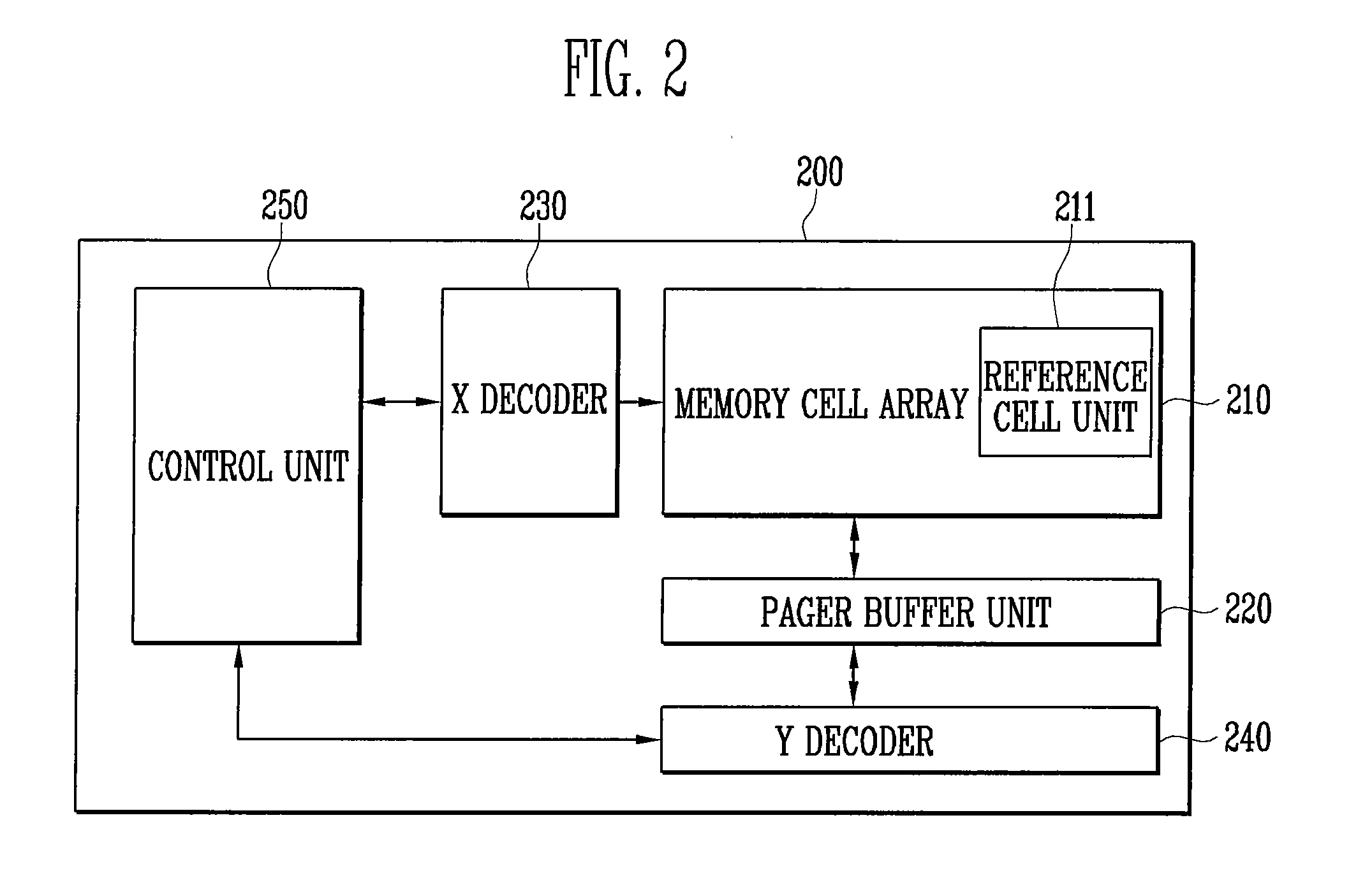
[0034]Referring to FIG. 2, a NAND flash memory 200 according to a first embodiment of the present invention includes a memory cell array 210 having memory cells for storing data, an X decoder 230 and a Y decoder 240 for selecting the memory cells of the memory cell array 210 in response to an input address, a page buffer unit 220 having page buffers for programming data into the memory cell array 210 or reading stored data, a control unit 250 for controlling programming and reading by controlling the memory cell array 210, the page buffer unit 220, the X decoder 230 and the Y decoder 240. It is to be noted that FIG. 2 only shows a partial construction of the NAND flash memory according to a first embodiment of the present invention.

[0035]The memory cell array 210 includes a plurality of blocks having a plurality of memory cells, and includes a reference cell unit ...


PUM


Abstract

A non-volatile memory device includes a memory cell array at least one block having a plurality of memory cells, and at least one reference cell with respect to each block, an X decoder and a Y decoder for selecting a memory cell for an operation according to an input address, a page buffer for programming data into a memory cell selected by the X decoder and the Y decoder or reading programmed data, and a controller for controlling the memory cell array, the X decoder, the Y decoder and the page buffers to calculate a change in a threshold voltage of the memory cells and compensate for a changed threshold voltage of a memory cell based on a change in a threshold voltage of the reference cell.

Description

CROSS-REFERENCES TO RELATED APPLICATIONS[0001]The present application claims priority to Korean patent application number 10-2006-134812, filed on Dec. 27, 2006, which is incorporated by reference in its entirety.BACKGROUND OF THE INVENTION[0002]The present invention relates to a non-volatile memory device and, more particularly, to a non-volatile memory device and a method to compensate for a threshold voltage shift.[0003]Flash memory that is non-volatile is classified into NAND flash memory or NOR flash memory. NOR flash memory has a structure in which memory cells are independently connected to a bit line and a word line and has a good random access temporal characteristic, whereas NAND flash memory has a structure in which a plurality of memory cells are connected in series, requiring only one contact per cell string, and is good in terms of the level of integration. Accordingly, the NAND structure is generally used in high-integrated flash memory.[0004]The well-known NAND flash...

Claims


Application Information

Patent Timeline
IPC IPC(8): G11C16/04G11C16/06
CPCG11C11/5628G11C11/5642G11C16/3431G11C16/3422G11C16/3418
Inventor KIM, KI SEOG
Owner SK HYNIX INC
Why Eureka
Try Eureka