
System and methods for driving an electro-optical device

a technology of electrooptical devices and driving methods, applied in the direction of static indicating devices, identification means, instruments, etc., can solve the problems of unobtainable desired display quality, and achieve the effect of good display quality display units

Inactive Publication Date: 2005-07-21
INTELLECTUAL KEYSTONE TECH LLC
View PDF8 Cites 22 Cited by
  • Summary
  • Abstract
  • Description
  • Claims
  • Application Information

AI Technical Summary

Benefits of technology

"The present invention provides an electronic circuit, a driving method, an electro-optical device, and an adjustment transistor that can reduce dispersion in the threshold voltages of transistors. This is achieved by including a first transistor, a second transistor, and a capacitive element in the circuit. The driving method includes a first step of electronically connecting the fourth terminal to a predetermined potential and a second step of changing the potential of the second electrode of the capacitive element from a second potential to a third potential to change the potential of the first control terminal. This can compensate for changes in manufacturing dispersion and maintain the desired potential. The electro-optical device includes a plurality of scanning lines, a plurality of data lines, a plurality of power lines, and a plurality of unit circuits with electro-optical elements. The invention provides a more stable and reliable electronic circuit that can reduce dispersion in threshold voltages and improve the performance of the electronic circuit."

Problems solved by technology

Especially when thin-film transistors are used as the driving transistors, a desired display quality may not be obtained because the thin-film transistors have much dispersion in their threshold voltages.

Method used


Image

  • System and methods for driving an electro-optical device
  • System and methods for driving an electro-optical device
  • System and methods for driving an electro-optical device

Examples


Embodiment Construction

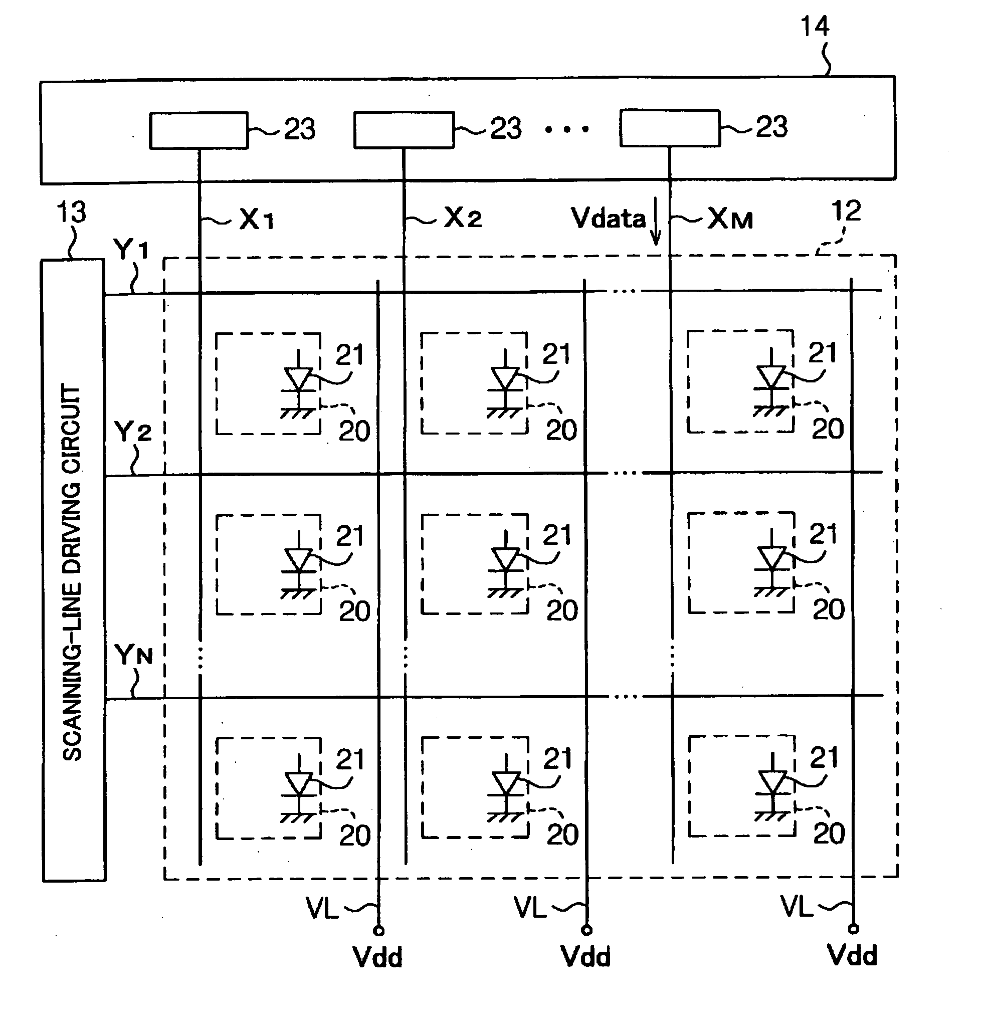
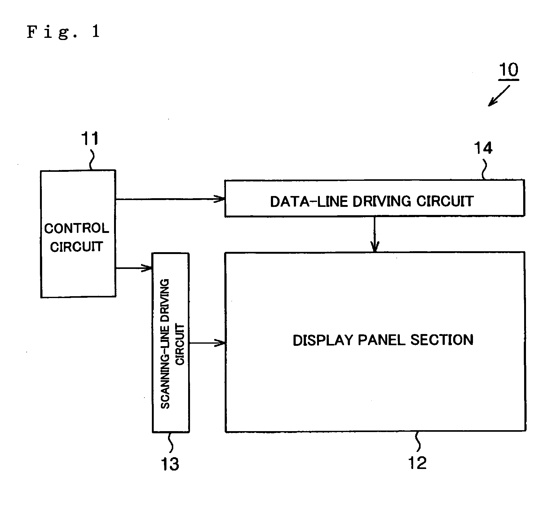
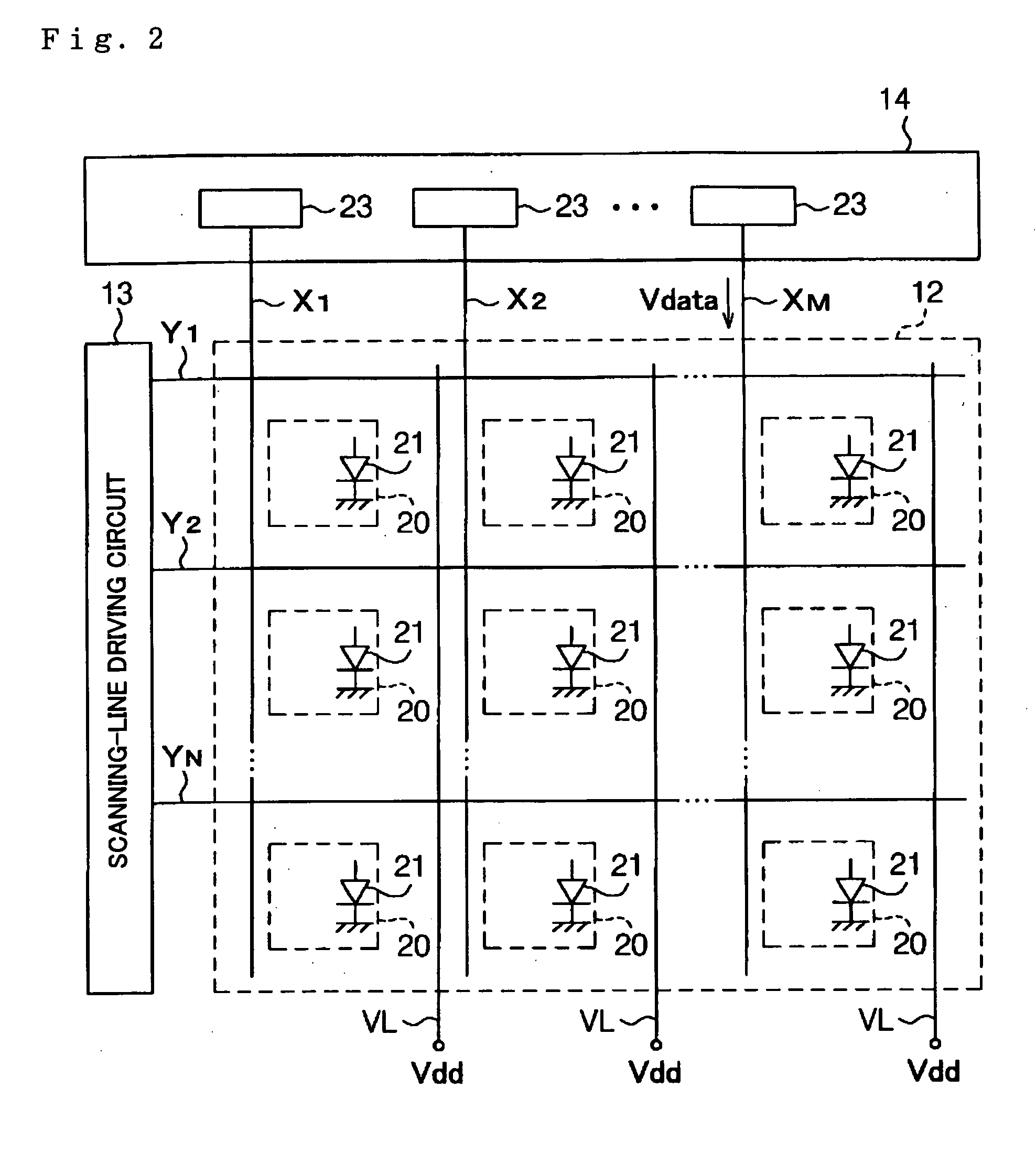
[0045] An organic EL display will be taken as an example of an electro-optical device according to an embodiment of the present invention and described by referring to FIG. 1 to FIG. 4. FIG. 1 shows the structure of the control block of the organic EL display. FIG. 2 is a block circuit diagram showing the internal circuit structure of a display panel section and a data-line driving circuit. FIG. 3 is a circuit diagram of a pixel circuit. FIG. 4 is a timing chart showing a driving method for the pixel circuit.

[0046] As shown in FIG. 1, the organic EL display 10 can include a control circuit 11, the display panel section 12, a scanning-line driving circuit 13, and the data-line driving circuit 14. The control circuit 11, the scanning-line driving circuit 13, and the data-line driving circuit 14 of the organic EL display 10 may be structured by independent electronic components. For example, each of the control circuit 11, the scanning-line driving circuit 13, and the data-line drivin...


PUM

PropertyMeasurementUnit
conduction stateaaaaaaaaaa
voltageaaaaaaaaaa
threshold voltageaaaaaaaaaa

Abstract

An electronic circuit, a driving method for an electronic circuit, an electro-optical device, a driving method for an electro-optical device, and an electronic apparatus are provided to reduce the dispersion of the threshold voltages of transistors. A driving transistor, first and second switching transistors, an adjustment transistor, a coupling capacitor, and a holding capacitor form a pixel circuit. The threshold voltage of the adjustment transistor is applied to the gate of the driving transistor. According to various embodiments, the luminance gradation of a display element, such as an organic EL element, can be precisely controlled according to a data voltage.

Description

CROSS REFERENCE TO RELATED APPLICATIONS [0001] This is a Divison of U.S. patent application Ser. No. 10 / 621,610 filed Jul. 18, 2003, which claims priority under 35 U.S.C. §119 of Japanese Patent Applications Nos. 2002-223160 filed Jul. 31, 2002 and 2003-198129 filed Jul. 16, 2003. The entire disclosures of the prior applications are hereby incorporated by reference herein in their entirety.BACKGROUND OF THE INVENTION [0002] 1. Field of Invention [0003] The present invention relates to electronic circuits, driving methods for electronic circuits, electro-optical devices, driving methods for electro-optical devices, and electronic apparatus. [0004] 2. Description of Related Art [0005] An active-matrix driving method is one of driving methods for electro-optical devices having electro-optical elements, such as liquid-crystal elements, organic EL elements, electro-phoresis elements, and electron-emission elements. In electro-optical devices which use the active-matrix driving method, a ...

Claims


Application Information

Patent Timeline
Patent Type & Authority Applications(United States)
IPC IPC(8): H01L51/50G02F1/133G09F9/30G09G3/00G09G3/20G09G3/30G09G3/32H01L27/12H01L27/32H01L29/04H01L29/10H01L29/786H01L29/80H01L31/036H01L31/0376H01L31/20H05B33/14
CPCG09G3/3233G09G2300/0819G09G2300/0852H01L27/12G09G2310/0262G09G2320/043G09G2310/0251G09G3/30
Inventor MIYAZAWA, TAKASHI
Owner INTELLECTUAL KEYSTONE TECH LLC
Learn More