Magnetoresistive effect element, magnetic memory element magnetic memory device and manufacturing methods thereof

a magnetic memory element and effect element technology, applied in the field of magnetic memory element, magnetic memory element, magnetic memory device and manufacturing methods, can solve the problems of inability to write so many times, wire breaking, and slow write speed, so as to improve the barkhausen noise, reduce the coercive force, and soft magnetic characteristics

Inactive Publication Date: 2007-08-28
SONY CORP
View PDF14 Cites 48 Cited by
  • Summary
  • Abstract
  • Description
  • Claims
  • Application Information

AI Technical Summary

Benefits of technology

[0073]A magnetoresistive effect element and a magnetic memory element according to the present invention have a ferromagnetic tunnel junction structure having a tunnel barrier layer sandwiched between at least a pair of ferromagnetic layers.
[0074]FIG. 1A is a schematic cross-sectional view of an example of a magnetoresistive effect element or a magnetic memory element 1 based upon a TMR element having this ferromagnetic tunnel junction structure. In this embodiment, an underlayer 3 is formed on a substrate, e.g. Si substrate, and an antiferromagnetic layer 4 is formed on the substrate through this underlayer 3. A ferromagnetic tunnel junction portion 8 on which a ferromagnetic layer 5 (hereinafter referred to as a “first ferromagnetic layer”), a tunnel barrier layer 6 and a ferromagnetic layer 7 (hereinafter referred to as a “second ferromagnetic layer”) are laminated in that order is formed on the antiferromagnetic layer.
[0075]Then, a protective layer 9 which might be called a top-coat layer is formed on this ferromagnetic tunnel junction portion 8.
[0076]The first ferromagnetic layer 5 is a magnetization fixed layer of which the magnetization direction is fixed, and the second ferromagnetic layer 7 is a magnetization free layer of which the magnetization direction is inverted, which is an information storage layer in the magnetic memory element.
[0077]This magnetization free layer or the second ferromagnetic layer 7 comprising the information storage layer has an amorphous or microcrystal structure in which the following alloy chemical elements were added to transition metals (hereinafter referred to as an “FMTM”) of at least one kind or more than two kinds of Fe, Ni, Co.
[0078]Since the magnetization free layer and the information storage layer based upon the ferromagnetic layer 7 has the amorphous or microcrystal structure as described above, it can decrease a coercive force while a spin polarizability of the FMTM is being maintained, it can obtain a soft magnetic characteristic to improve a Barkhausen noise in an R—H curve and a rectangle property, it can serve as the information storage layer to decrease dispersions in writing information when the magnetic field is inverted repeatedly and therefore can obtain satisfactory write characteristics. At the same time, it can realize a high TMR ratio and can obtain excellent read characteristics in which a bias dependence characteristic has been improved.

Problems solved by technology

However, the flash memory encounters with a drawback that its write speed is as slow as the microsecond order.
On the other hand, it is pointed out that the FRAM has a problem in which it cannot be rewritten so many times.
There is then a risk that breaking of wire will be caused by electromigration.
If the magnetic characteristic of the magnetic memory element is dispersed at every element and the magnetic characteristic is dispersed when the same element is used repeatedly, the selective writing using the asteroid characteristic becomes difficult.

Method used


Image

  • Magnetoresistive effect element, magnetic memory element magnetic memory device and manufacturing methods thereof
  • Magnetoresistive effect element, magnetic memory element magnetic memory device and manufacturing methods thereof
  • Magnetoresistive effect element, magnetic memory element magnetic memory device and manufacturing methods thereof

Examples


##ventive example 1

INVENTIVE EXAMPLE 1

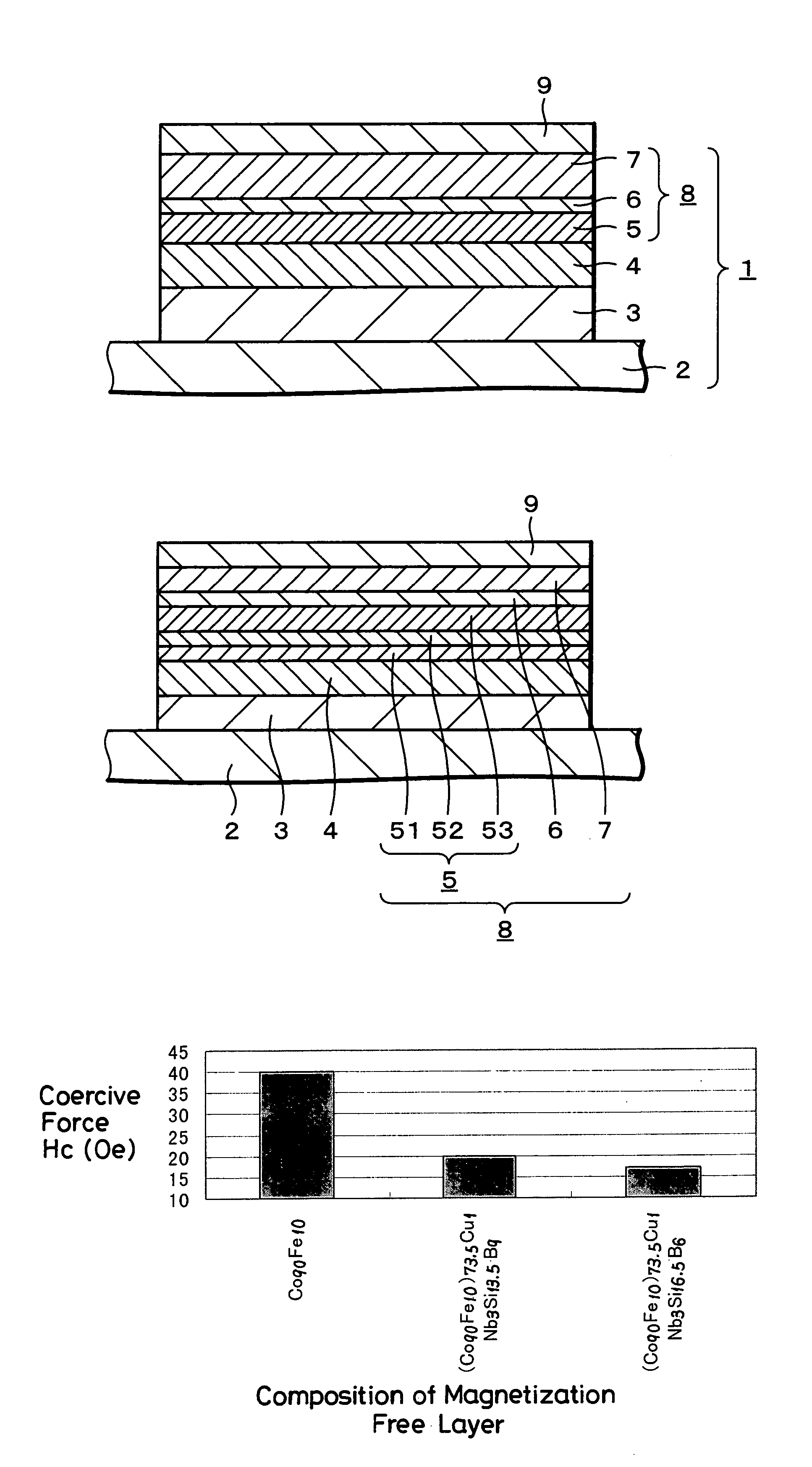
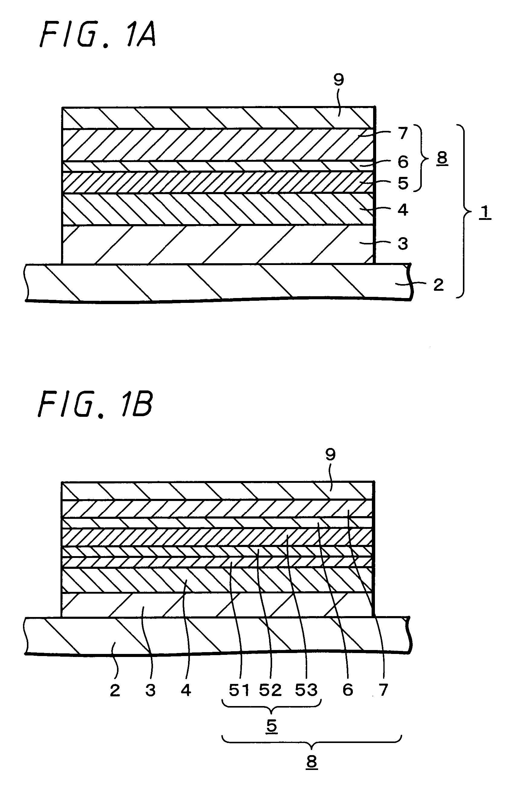
[0139]A magnetic memory element according to this inventive example was formed as a TMR element including a ferromagnetic tunnel junction portion having a fundamental structure based upon a lamination layer of the aforementioned ferromagnetic material layer 5 / tunnel barrier layer 6 / ferromagnetic material layer 7, i.e., MTJ (Magnetic Tunnel. Junction).

[0140]In this case, the first ferromagnetic layer5 is formed so as to have a lamination layer ferri structure.

[0141]Moreover, in this case, as in the spin-valve type memory, the ferromagnetic layer 5 is formed as the magnetization fixed layer, of which the magnetization direction is fixed by the antiferromagnetic layer 4 so that the direction of the magnetization is constantly set to be constant. The other ferromagnetic layer 7 is formed as the magnetization free layer, i.e., the information storage layers so that the direction of the magnetization is inverted with application of external magnetic fields.

[0142]In this...

##ventive example 2

INVENTIVE EXAMPLE 2

[0153]In the film arrangement of the TMR element 1, except that the composition of the second ferromagnetic layer 7, i.e., the magnetization free layer (information storage layer) was selected to be (Co90Fe10)75Si15Ml10 and that Ml was selected to be B, C, P, Al, this inventive example had a similar arrangement to that of the inventive example 1.

##ventive example 3

INVENTIVE EXAMPLE 3

[0154]In the film arrangement of the TMR element 1, except that the composition of the second ferromagnetic layer 7, i.e., the magnetization free layer (information storage layer) was selected to be (Co90Fe10)80B20, (Co75Fe25)80B20, (Co50Fe50)80B20, (Ni80Fe20)80B20, this inventive example had a similar arrangement to that of the inventive example 1.


PUM

PropertyMeasurementUnit
magnetizationaaaaaaaaaa
current densityaaaaaaaaaa
temperatureaaaaaaaaaa

Abstract

In a magnetoresistive effect element using a ferromagnetic tunnel junction having a tunnel barrier layer sandwiched between at least a pair of ferromagnetic layers, a magnetization free layer comprising one of the ferromagnetic layers is composed of a single layer of a material having an amorphous or microcrystal structure or a material layer the main portion of which has an amorphous or microcrystal structure. The magnetoresistive effect element can produce excellent magnetic-resistance characteristics, and a magnetic memory element and a magnetic memory device using the magnetoresistive effect element as a memory element thereof can improve both of write and read characteristics at the same time.

Description

BACKGROUND OF THE INVENTION[0001]The present invention relates to a magnetoresistive effect element, a magnetic memory element, a magnetic memory device and manufacturing methods thereof, and particularly to a magnetoresistive effect element having stable magnetic characteristics, a magnetic memory element operable as a magnetic nonvolatile memory element, a magnetic memory device composed of the magnetic memory element and manufacturing methods thereof.[0002]As information communication devices, in particular, personal small devices such as personal digital assistants are making great spread, elements such as memories and logics comprising information communication device are requested to have higher performance such as higher integration degree, higher operation speed and lower power consumption. In particular, technologies for making nonvolatile memories become higher in density and larger in storage capacity are progressively increasing their importance as technologies for repla...

Claims


Application Information

Patent Timeline
Patent Type & Authority Patents(United States)
IPC IPC(8): H01L21/00G11B5/127G11B5/33G01R33/09G11B5/39G11C11/15G11C11/16H01F10/32H01F41/18H01F41/30H01L21/8246H01L27/22H01L43/10H01L43/12
CPCB82Y10/00B82Y25/00B82Y40/00G01R33/093G11B5/3903G11B5/3909G11C11/15G11C11/16H01F10/3204H01F10/3254H01F41/302H01L27/228H01L43/10H01L43/12G11C2029/5002H01F41/18G11C11/1659G11C11/161G11C11/1657H10B61/22H10N50/85H10N50/01
Inventor OHBA, KAZUHIROHAYASHI, KAZUHIKOKANO, HIROSHIBESSHO, KAZUHIROMIZUGUCHI, TETSUYAHIGO, YUTAKAHOSOMI, MASANORIYAMAMOTO, TETSUYANARISAWA, HIROAKISONE, TAKEYUKIENDO, KEITAROKUBO, SHINYA
Owner SONY CORP
Why Eureka
Try Eureka