Pixel and organic light emitting display using the same

a technology of organic light and display, applied in the direction of identification means, instruments, static indicating devices, etc., can solve the problems of non-uniform display, deterioration of yield, and complex structure of pixel, and achieve the effect of simplifying the structure of pixel

a technology of organic light and display, applied in the direction of identification means, instruments, static indicating devices, etc., can solve the problems of non-uniform display, deterioration of yield, and complex structure of pixel, and achieve the effect of simplifying the structure of pixel

US20130222356A1Active Publication Date: 2013-08-29SAMSUNG DISPLAY CO LTD +1

Image

  • Pixel and organic light emitting display using the same
  • Pixel and organic light emitting display using the same
  • Pixel and organic light emitting display using the same

Examples


first embodiment

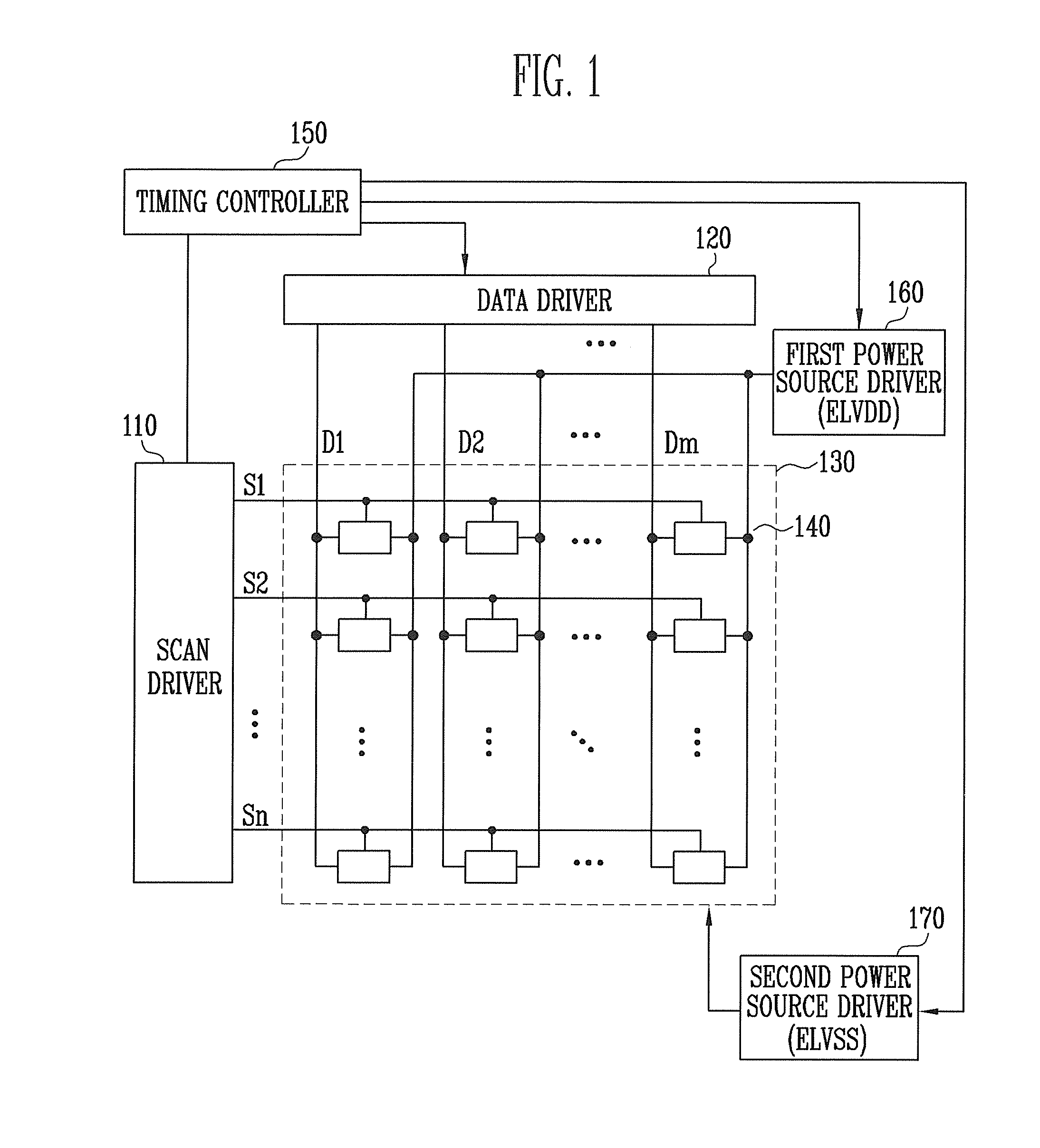
[0037]FIG. 1 is a view illustrating an organic light emitting display according to the present invention.

[0038]Referring to FIG. 1, the organic light emitting display according to the first embodiment of the present invention includes a display unit 130 including pixels 140 positioned at the crossing regions of scan lines S1 to Sn and data lines D1 to Dm, a scan driver 110 for driving the scan lines S1 to Sn, a data driver 120 for driving the data lines D1 to Dm, a first power source driver 160 for supplying a first power source ELVDD to the pixels 140, a second power source driver 170 for supplying a second power source ELVSS to the pixels 140, and a timing controller 150 for controlling the drivers 110, 120, 160, and 170.

[0039]Each of the pixels 140 is coupled to a data line (one of D1 to Dm), a scan line (one of S1 to Sn), the first power source ELVDD, and the second power source ELVSS. Each of the pixels 140 controls the amount of current that flows from the relatively high leve...

second embodiment

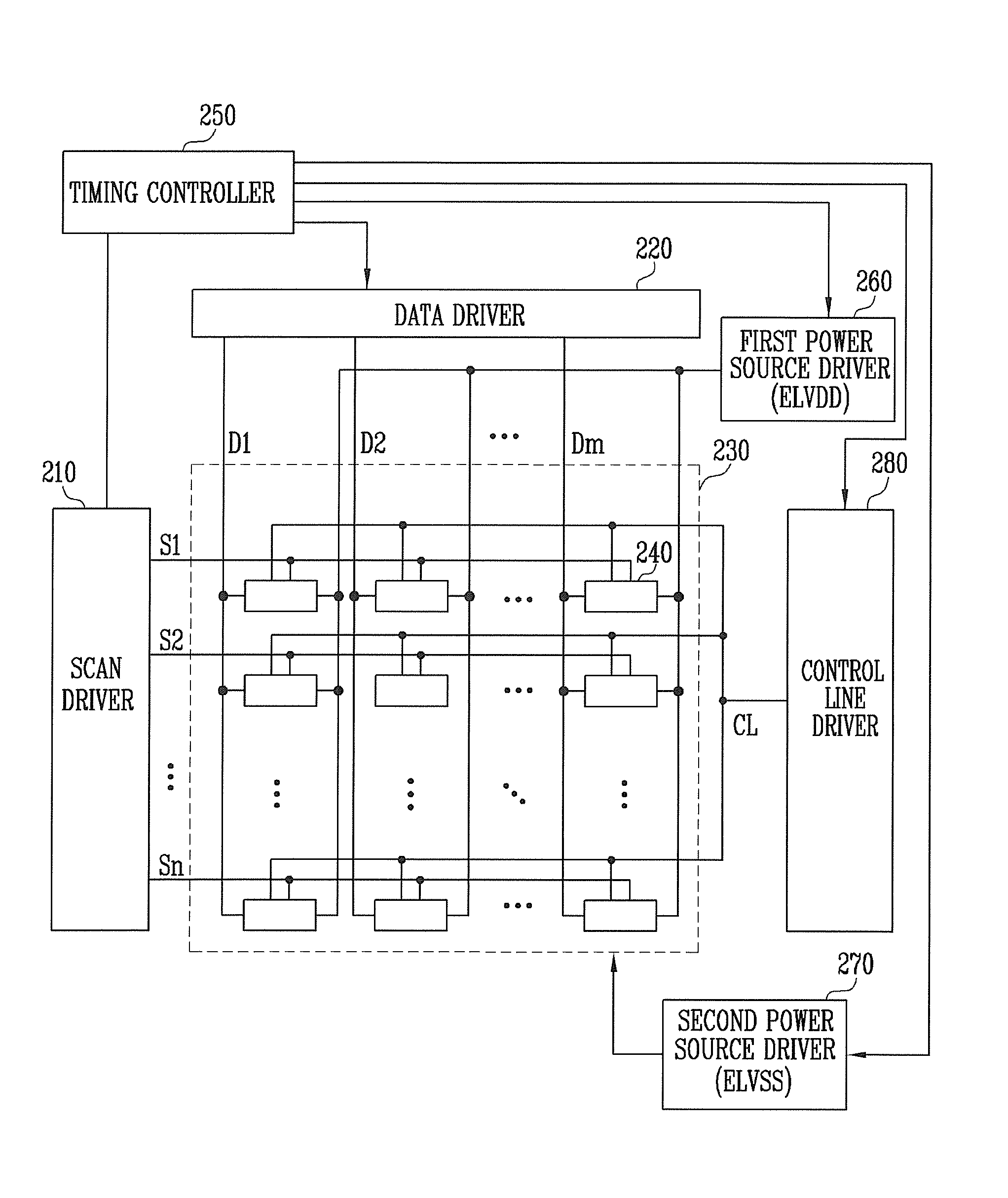
[0067]FIG. 4 is a view illustrating an organic light emitting display according to the present invention.

[0068]Referring to FIG. 4, the organic light emitting display according to the second embodiment of the present invention includes a display unit 230 including pixels 240 positioned at the crossing regions of scan lines S1 to Sn, data lines D1 to Dm, and a control line CL, a scan driver 210 for driving the scan lines S1 to Sn, a data driver 220 for driving the data lines D1 to Dm, a control line driver 280 for driving the control line CL, a first power source driver 260 for supplying a first power source ELVDD to the pixels 240, a second power source driver 270 for supplying a second power source ELVSS to the pixels 240, and a timing controller 250 for controlling the drivers 210, 220, 260, 270, and 280.

[0069]Each of the pixels 240 is coupled to the data line (one of D1 to Dm), the scan line (one of S1 to Sn), the control line CL, the first power source ELVDD, and the second powe...


PUM


Abstract

A pixel having a simplified structure can compensate for the threshold voltage of a driving transistor thereof. The pixel includes an organic light emitting diode (OLED) having a cathode electrode coupled to a second power source, a storage capacitor coupled between a data line and a first node, a second transistor having a first electrode coupled to a first power source, a second electrode coupled to an anode electrode of the OLED, and a gate electrode coupled to the first node, a first transistor coupled between the first node and the second electrode of the second transistor, a gate electrode of the first transistor being coupled to a current scan line, and a third transistor coupled between the second electrode of the second transistor and the anode electrode of the OLED, a gate electrode of the third transistor being coupled to a control line.

Description

CROSS-REFERENCE TO RELATED APPLICATION[0001]This application claims priority to and the benefit of Korean Patent Application No. 10-2012-0020260, filed on Feb. 28, 2012, in the Korean Intellectual Property Office, the entire content of which is incorporated herein by reference.BACKGROUND[0002]1. Field[0003]The present invention relates to a pixel and an organic light emitting display using the same, and more particularly, to a pixel capable of simplifying the structure thereof and an organic light emitting display using the same.[0004]2. Description of the Related Art[0005]In general, a pixel of an organic light emitting display includes a thin film transistor (TFT) and a capacitor. The TFT includes a semiconductor layer for providing a channel region and source and drain regions, a gate electrode provided on the semiconductor layer of the channel region and electrically insulated from the semiconductor layer by a gate insulating layer, and source and drain electrodes respectively c...

Claims


Application Information

Patent Timeline
29 Aug 2013
Publication
US20130222356A1
IPC
G09G5/00; H01L33/08
CPC
G09F9/33; G09G3/3233; G09G2300/0866; G09G2300/0842; G09G2300/0861; G09G2300/0819; G09G3/3208; H10K59/1216
Inventors
JEONG, JIN-TAE; KWON, OH-KYONG