Multi-input/output repair method of NAND flash memory device and NAND flash memory device thereof

a multi-input/output repair and memory device technology, applied in the field of multi-input/output repair of nand flash memory device thereof, can solve the problems of complex circuit and impossible repair

Inactive Publication Date: 2006-04-11
STMICROELECTRONICS SRL +1
View PDF3 Cites 50 Cited by
  • Summary
  • Abstract
  • Description
  • Claims
  • Application Information

AI Technical Summary

Benefits of technology

[0006]Accordingly, the present patent addresses the above problems, and provides a NAND flash memory device in which multi-I / O repair is possible.

Problems solved by technology

However, if two or more failed columns have the M number of different I / Os while having the same address, repair is impossible.
This results in a complicated circuit.

Method used


Image

  • Multi-input/output repair method of NAND flash memory device and NAND flash memory device thereof
  • Multi-input/output repair method of NAND flash memory device and NAND flash memory device thereof
  • Multi-input/output repair method of NAND flash memory device and NAND flash memory device thereof

Examples


Embodiment Construction

[0016]Various embodiments will be described below with reference to the accompanying drawings. Those of ordinary skill in the art will appreciate that the disclosed embodiments may be modified in various manners and the scope of the present patent is not limited by the embodiments disclosed.

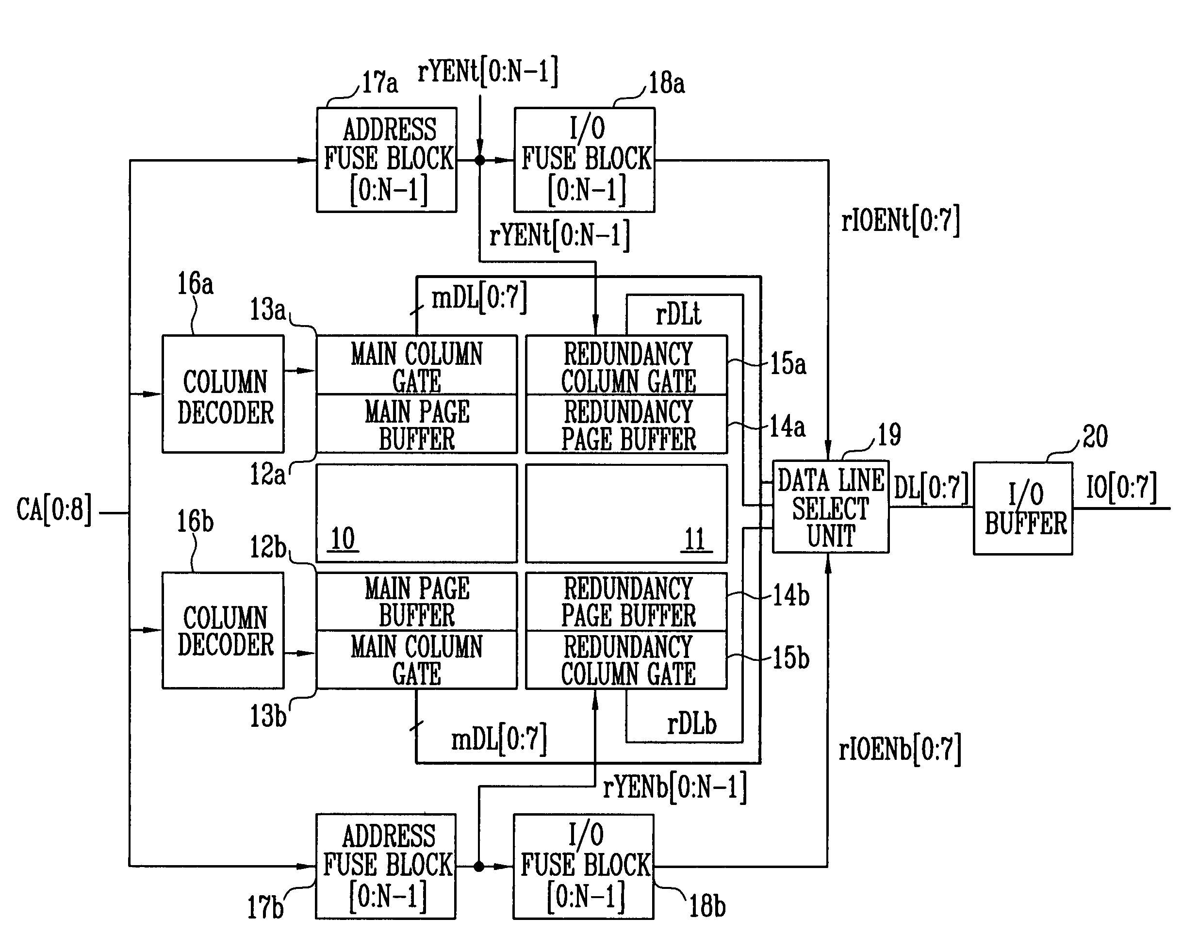
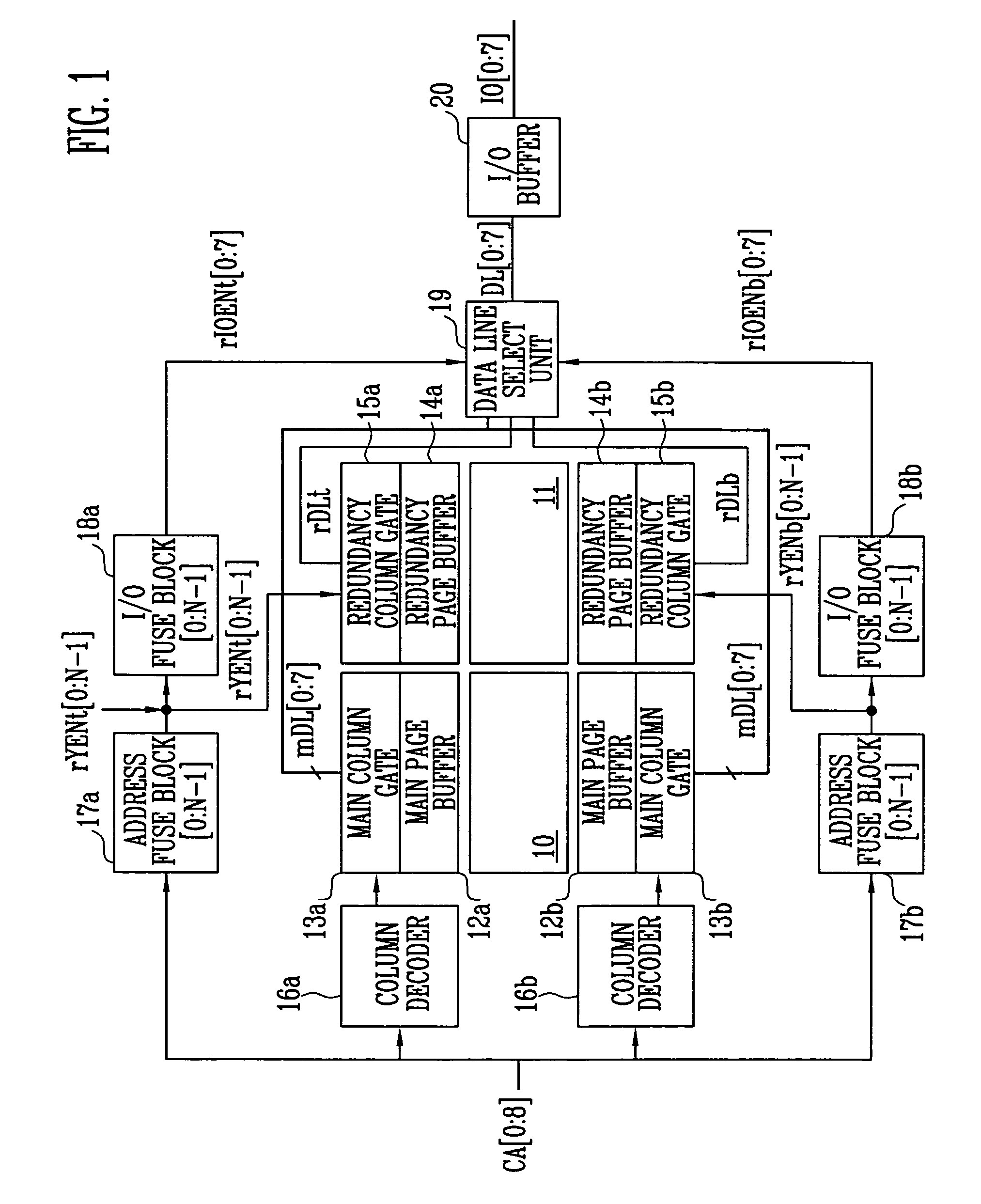
[0017]FIG. 1 is block diagram illustrating the construction of a NAND flash memory device

[0018]Referring to FIG. 1, the NAND flash memory device includes a main array 10 and a redundancy array 11. The main array 10 and the redundancy array 11 are composed of a number of strings. To each of the strings is serially connected a number of cells (e.g., 16 or 32 in number).

[0019]Main page buffers 12a,12b and main column gates 13a,13b are positioned at the top and bottom of the main array 10. In the similar manner, redundancy page buffers 14a,14b and redundancy column gates 15a,15b are positioned even at the top and bottom of the redundancy array 11. The main page buffers 12a, 12b are selected by addres...


PUM


Abstract

A multi-I / O repair method of a NAND flash memory device and a NAND flash memory device thereof are disclosed. A NAND flash memory device is disclosed in which page buffers are positioned at the top and bottom of a main array and a redundancy array and have different data lines. The top / bottom page buffers of the redundancy array are all selected according to an external address and data is transmitted over redundancy data lines, and this data is finally selected through a data line select unit. Accordingly, if main columns having different addresses are to be repaired, they can be replaced with redundancy columns one to one and multi-I / O repair of two main columns having the same address is thus possible.

Description

[0001]This application relies for priority upon Korean Patent Application No. 2004-0033206 filed May 11, 2004, the contents of which are herein incorporated by reference in their entirety.BACKGROUND[0002]1. Field of the Invention[0003]The present patent relates to a multi-input / output repair method of a NAND flash memory device and NAND flash memory device thereof, and more specifically, to a NAND flash memory device in which multi-I / O repair is possible by minimizing increases in the area due to increased circuits.[0004]2. Discussion of Related Art[0005]In semiconductor memory devices, an input / output (I / O) repair method can increase repair efficiency in such a manner that failed columns of a main array are replaced with redundancy columns one to one. However, if two or more failed columns have the M number of different I / Os while having the same address, repair is impossible. In order for such repair to be possible, the M number of redundancy blocks is required and additional circ...

Claims


Application Information

Patent Timeline
Patent Type & Authority Patents(United States)
IPC IPC(8): G11C16/00G11C16/04G11C11/34G11C16/02G11C16/06G11C29/00G11C29/04
CPCG11C29/846G11C16/0483A44C3/00A44C5/20A44C15/005A44D2203/00B21L11/005
Inventor PARK, JIN SU
Owner STMICROELECTRONICS SRL
Why Eureka
Try Eureka