Semiconductor integrated circuit and memory checking method

a technology of integrated circuits and integrated circuits, which is applied in the direction of digital computers, instruments, digital storage, etc., can solve the problems of increasing the area required for circuits, increasing the time required for checking, and reducing the accuracy of the test, so as to prevent the leakage of secret data and shorten the check time

Inactive Publication Date: 2010-08-24
PANASONIC CORP
View PDF13 Cites 1 Cited by
  • Summary
  • Abstract
  • Description
  • Claims
  • Application Information

AI Technical Summary

Benefits of technology

[0017]According to the semiconductor integrated circuit, the memory can be initialized without providing an initialization dedicated circuit for initializing the memory and the memory can be accessed from the outside only after completely erasing secret data within the memory. Thus, a circuit area necessary for the initialization dedicated circuit can be eliminated and the leakage of secret data can be prevented.
[0019]Thus, even if a normal user tries to access the memory for secret data, since the normal user can merely access the another memory, the leakage of secret data can be prevented.
[0021]Thus, even if a normal user tries to access the memory for secret data, since the normal user can merely access redundant area, the leakage of the secret data can be prevented. Further, the redundant area can be checked and evaluated.
[0023]Thus, when the reading operation is tried by the scanning, which necessarily results in the writing operation to the memory, and so the secret data is rewritten and the leakage of the secret data can be prevented. In this manner, the leakage of the secret data using the scanning chain and the observation flip-flop can be prevented.
[0031]Thus, it is unnecessary to initialize secret data stored in the memory before performing the checking by the path for the memory isolation test from the external terminal. Further, at the time of checking the memory, even if a failure is found after performing the checking by the path for the memory isolation test from the external terminal, when the failure can be repaired by using a redundant memory, it is unnecessary to perform the initializing operation dedicated for the secret data stored in the memory. In this manner, since the process of the initialization can be eliminated by initializing the secret data memory using the memory BIST, the checking time can be shortened. Further, the repair of the memory is made possible.
[0032]According to the semiconductor integrated circuit and the memory checking method of the invention, secret data can be erased without providing an initialization dedicated circuit for initializing the memory, and the memory can be accessed from the outside only after completely erasing the secret data. Thus, a circuit area necessary for the initialization dedicated circuit can be eliminated and the leakage of secret data can be prevented.

Problems solved by technology

However, in the aforesaid semiconductor integrated circuit, in the case of the memory for storing secret data, a test dedicated terminal can not be provided at the outside thereof directly.
However, the initialization dedicated circuit for completely initializing the secret data results in the increase of an area required for the circuits.
Further, in the case of a memory having a redundancy survival function using the laser repair, since the initialization using a dedicated circuit and an individual test using the isolation are required, a time required for the checking becomes long.

Method used


Image

  • Semiconductor integrated circuit and memory checking method
  • Semiconductor integrated circuit and memory checking method
  • Semiconductor integrated circuit and memory checking method

Examples


first embodiment

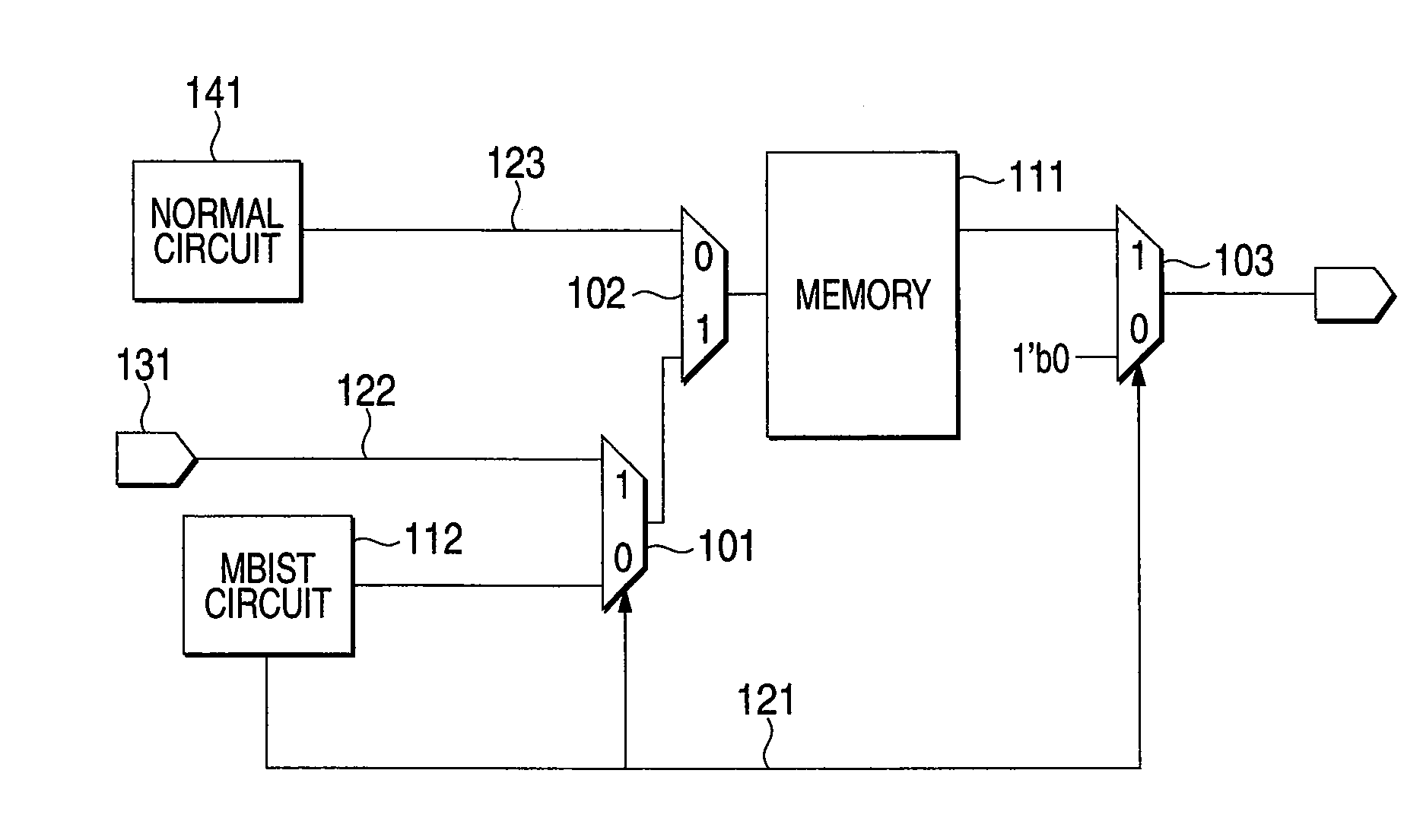
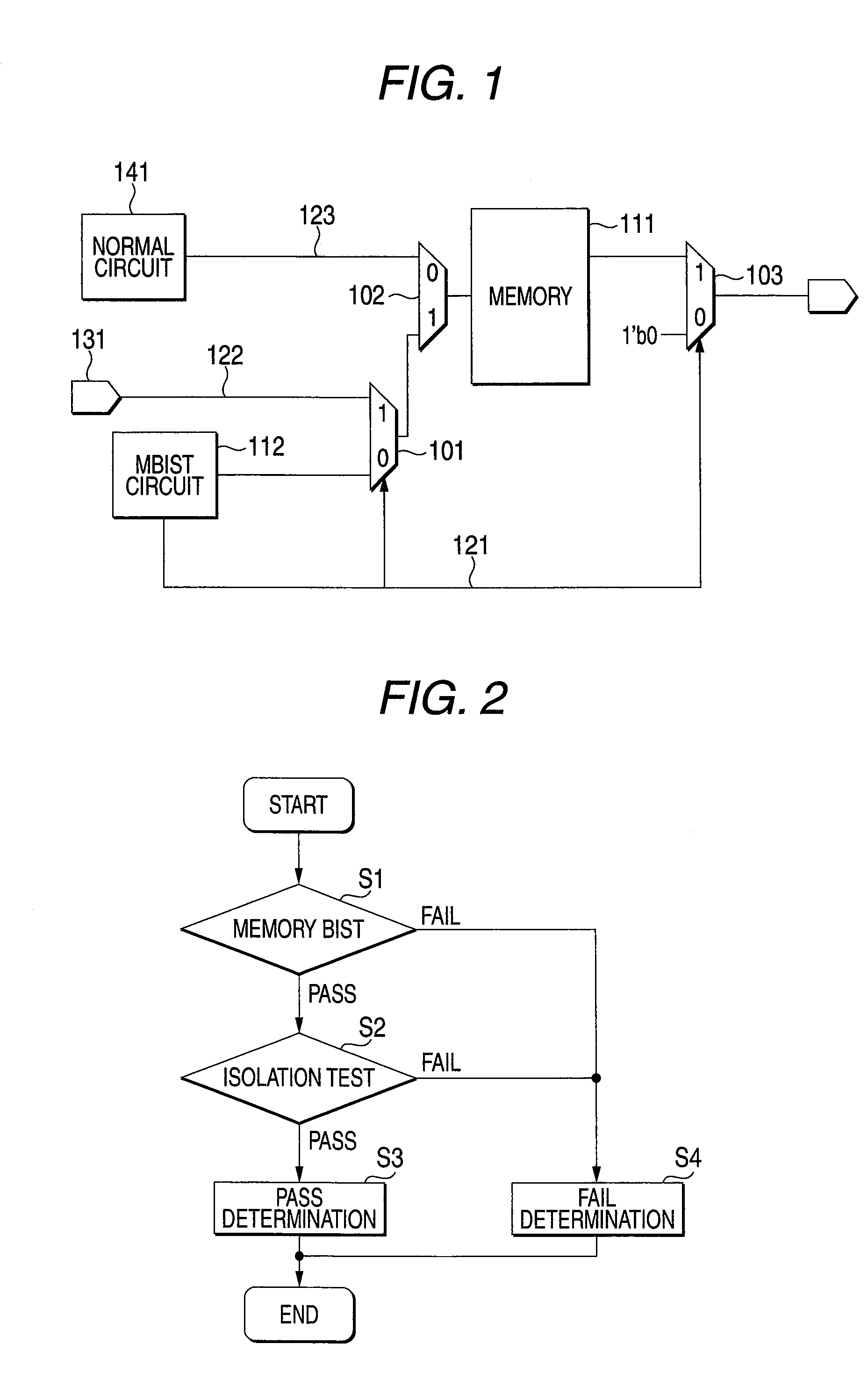
[0042]FIG. 1 is a block diagram showing a semiconductor integrated circuit according to the first embodiment. As shown in FIG. 1, the semiconductor integrated circuit according to the first embodiment includes a first selector 101 for switching between a path from a memory BIST (MBIST) circuit 112 and a direct input path 122 from an external terminal 131, a selector 102 for switching between the direct input path 122 from the external terminal 131 and a path 123 from a normal circuit 141, and a selector 103 for switching between an output path from a memory 111 and a path to which a pseudo signal is inputted. The selector 103 receives a check completion signal 121 from the MBIST circuit 112 as a selection signal. The memory 111 is configured by an SRAM and stores secret data therein.

[0043]The memory check operation performed by the semiconductor integrated circuit according to the first embodiment will be explained. FIG. 2 is a flowchart showing the memory check procedure. First, th...

second embodiment

[0047]In a memory mounting a redundant memory area, in the case where a failure portion is detected in a using memory area, the failure memory can be repaired by utilizing the redundant memory area. The second embodiment shows a case where a secret data memory includes the redundant memory area. Since the configuration of the semiconductor integrated circuit according to the second embodiment is same as that of the first embodiment, portions identical to those of the first embodiment are referred to by the common symbols, with explanation thereof being omitted.

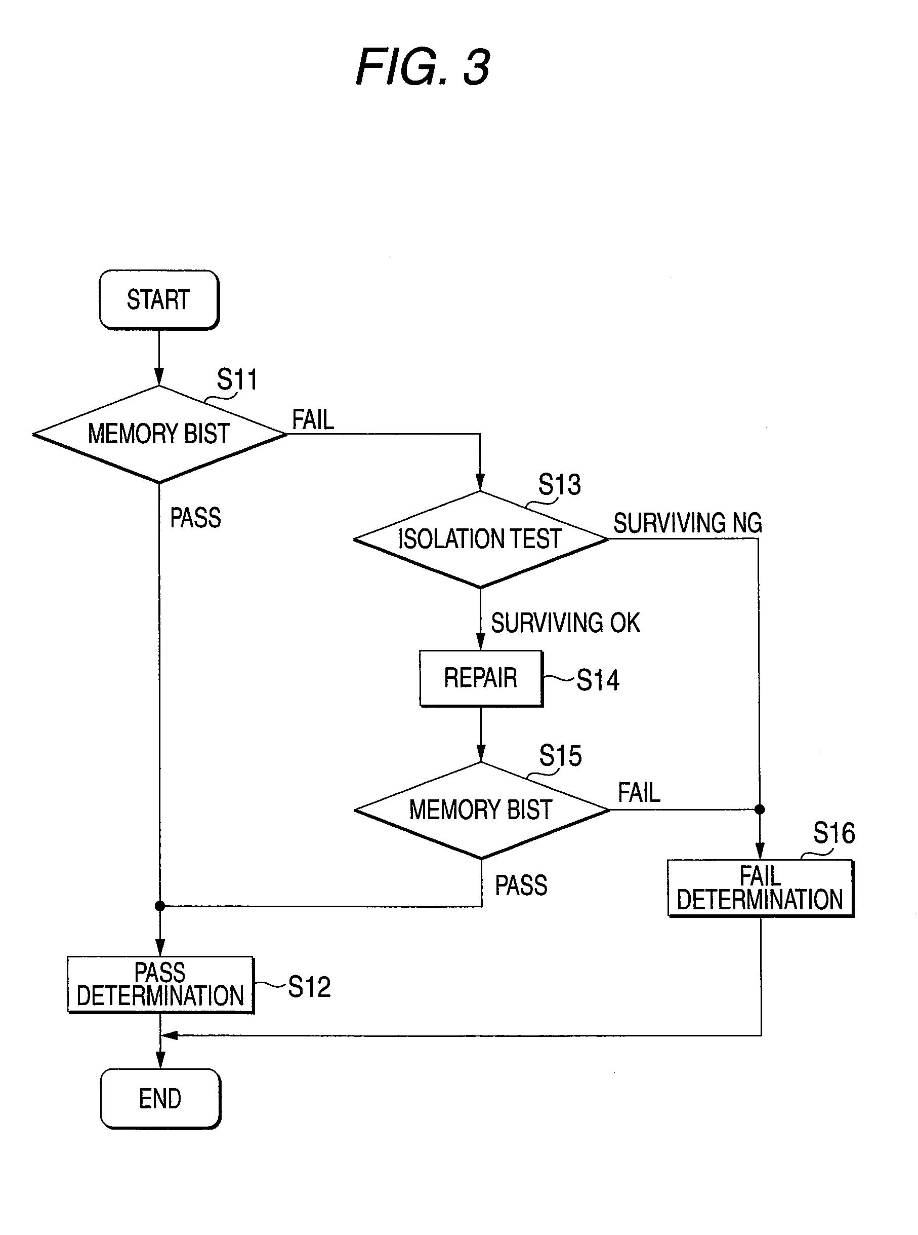
[0048]FIG. 3 is a flowchart showing the memory checking procedure in the case of repairing the memory. First, the MBIST circuit 112 executes the memory BIST (built in self test) with respect to the memory 111 having the redundant memory area and determines the result of the test (step S11). When the execution of the memory BIST results in success (PASS), the PASS determination is made (step S12) and the test is completed.

[0049...

third embodiment

[0052]FIG. 4 is a block diagram showing the semiconductor integrated circuit according to the third embodiment. In the figure, portions identical to those of the first embodiment are referred to by the common symbols, with explanation thereof being omitted. In the semiconductor integrated circuit according to the third embodiment, a memory (pseudo memory) 513 for normal data is mounted separately from the memory 111 for secret data. The selector 103 switches between the output of the memory 111 and the output of the pseudo memory 513.

[0053]According to the semiconductor integrated circuit of the third embodiment, at the time of executing the isolation test via the external terminal 131, the selector 103 is switched so that the value of the pseudo memory 513 is outputted until the initialization is completed. Thus, even when a usual user tries to access the secret data memory, since the usual user can access only to the pseudo memory, the leakage of the secret data can be prevented.

[...


PUM


Abstract

The semiconductor integrated circuit includes a memory for storing secret data, a memory BIST circuit for executing a memory. BIST, a first selector for switching between a path for a memory isolation test via an external terminal and a path from the memory BIST circuit, a second selector for switching between a path from the output of the first selector and a path from a normal circuit and having an output coupled to the memory, and a third selector for switching between a path from the output of the memory and a path for receiving a pseudo signal and receiving a check completion signal outputted from the memory BIST circuit as a selection signal. In this semiconductor integrated circuit, after the memory is initialized by executing the memory BIST, the memory can be accessed from the external terminal via the path for the memory isolation test.

Description

BACKGROUND OF THE INVENTION[0001]1. Field of the Invention[0002]The present invention relates to a semiconductor integrated circuit and a method of checking a memory.[0003]2. Description of the Related Art[0004]Conventionally, a semiconductor integrated circuit includes an initialization dedicated circuit for completely initializing secret data. In the case of checking or evaluating a memory for storing the secret data, the accessing to the memory is allowed after the initialization dedicated circuit completely initializes the memory. FIG. 8 is a block diagram showing a semiconductor integrated circuit of the related art. In the semiconductor integrated circuit shown in FIG. 8, in the case of executing an isolation test from an external terminal 241, it is required to initialize a memory 211 by an initializing circuit 213.[0005]Another semiconductor integrated circuit of the related art includes a circuit for determining whether or not an access is allowed thereby to control the acc...

Claims


Application Information

Patent Timeline
Patent Type & Authority Patents(United States)
IPC IPC(8): G11C29/12G06F21/60G06F21/62
CPCG11C29/46G11C2029/0407
Inventor YAMAGUCHI, TOKUSHISEKIGUCHI, HIROYUKISHIOTA, RYOJINAKANO, MITSUYA
Owner PANASONIC CORP
Why Eureka
Try Eureka