Cycle independent data to echo clock tracking circuit

a clock tracking and cycle independent technology, applied in the direction of digital storage, generating/distributing signals, instruments, etc., can solve the problems of memory bottleneck, memory is a well known limitation of computer system performance, drams are relatively inexpensive to fabricate but are slow as compared to srams,

Inactive Publication Date: 2000-10-17
IBM CORP
View PDF6 Cites 82 Cited by
  • Summary
  • Abstract
  • Description
  • Claims
  • Application Information

AI Technical Summary

Problems solved by technology

Random access memory (RAM) performance is a well known limitation to computer system performance.
This is almost never the case and, so, the memory is a system bottleneck.
DRAMs are relatively inexpensive to fabricate but are slow as compared to SRAMS.
One drawback to the DDR architecture is that processors have to modify their cache control logic to recognize the double-data-rate signal.
The loss of tracking between echo clocks and data, will result in specification violations between memory devices and microprocessor (or vice-versa).
Further loss of tracking will result in data glitches that can cause system failures.

Method used


Image

  • Cycle independent data to echo clock tracking circuit
  • Cycle independent data to echo clock tracking circuit
  • Cycle independent data to echo clock tracking circuit

Examples


Embodiment Construction

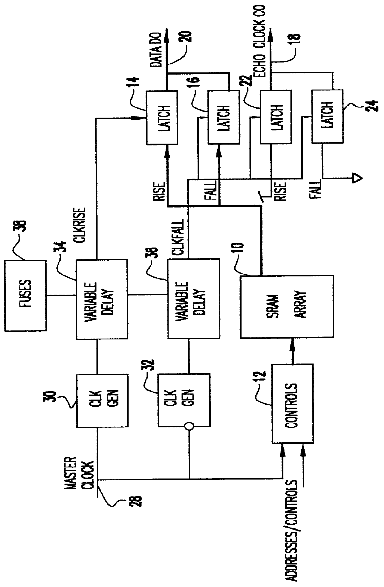
Referring now to the drawings, and more particularly to FIG. 1, there is shown a double data rate (DDR) SRAM with an echo clock controlled by a fuse circuit. An SRAM 10 comprises an array of addressable memory locations accessible by the memory controller 12. Data from the SRAM array 10 is divided into two groups, rise data and fall data. The rise data is latched through to a microprocessor input buffer (not shown)via latch 14 and, similarly the fall data is latched via the latch 16. Each is clocked by CLKRISE / CLKFALL of the following cycle. Latches 22 and 24 are also latched by CLKRISE / CLKFALL, respectively, to output an echo clock signal 18. In this manner the echo clock signal 18 tracks the data signal 20. That is, the echo clock signal 18 tracks the data output from the latches 14 and 16 to indicate when a valid data is available on the data line 20. The input of latch 22 is tied to a voltage high while the input of latch 24 is tied to a voltage low. A master clock signal 28 dri...


PUM


Abstract

A comparator and variable delay circuit are provided to maintain the tracking between data and echo clocks in a double data rate (DDR)RAM device. This is accomplished by providing a global data signal (dummy data signal) that tracks with the actual memory array data. This global data signal is compared to the timing of the RAM clock (CLOCK) to determine a delay time between the two by which the pipeline clocks (CLKRISE/CLKFALL) must be delayed. As a result, the pipeline clocks are pushed out as needed so that they always transition after the array data arrives at the output latch. Therefore, as cycle time decreases, both echo clocks and data are pushed out identically and maintain their required tracking.

Description

1. Field of the InventionThe present invention generally relates to random access memory (RAM) devices and, more particularly, to an echo clock tracking circuit for tracking data output from a double data rate (DDR) RAM device.2. Description of the Related ArtRandom access memory (RAM) performance is a well known limitation to computer system performance. Processor speeds are rapidly outpacing primary memory performance, with both processor designers and system manufacturers developing higher performance memory subsystems in an effort to minimize memory performance limitations. Ideally, the memory performance would match or exceed processor performance, i.e., a memory cycle time would be less than one processor clock cycle. This is almost never the case and, so, the memory is a system bottleneck.There are two common families of RAM memory devices used as primary storage directly accessible by the microprocessor. The first, static random access memory devices (SRAMS) are based on fli...

Claims


Application Information

Patent Timeline
Patent Type & Authority Patents(United States)
IPC IPC(8): G11C7/22G11C7/10G11C7/00G06F1/10G11C11/413G06F12/00G11C11/407
CPCG11C7/1051G11C7/106G11C7/222G11C7/22G11C7/1066G11C7/00
Inventor PILO, HAROLDCOVINO, JAMES J.
Owner IBM CORP
Why Eureka
Try Eureka