8T SRAM cell with higher voltage on the read WL

a sram cell and read current technology, applied in the field of improved stability of sram memory cells, can solve the problems of limiting the ability of the designer to increase the read performance, becoming increasingly difficult to design an sram cell, and changing the state of the memory cell, so as to achieve the effect of concurrent optimization of the read current and stability of the cell and not consuming unnecessary supply power

Active Publication Date: 2007-12-06
TEXAS INSTR INC
View PDF8 Cites 82 Cited by
  • Summary
  • Abstract
  • Description
  • Claims
  • Application Information

AI Technical Summary

Benefits of technology

[0015]The read buffer circuit is configured to permit a dedicated read word line (RWL) for read operations and a separate write word line (WWL) for accessing the core cell during write operations. Accordingly, the independent read and write word lines permit different voltages on the read word line RWL and write word line WWL for optimizing read current while avoiding data upsets. For example, a relatively higher voltage may be used on the RWL to obtain more read current, and a relatively lower voltage on the WWL to avoid upsets.
[0020]The SRAM memory cell structure of the present invention allows independent optimization of the static noise margin, trip voltage, and read current, thereby avoiding some of the static noise margin and trip voltage problems of conventional SRAM cells (e.g., a conventional 6T differential cell). The structures described herein are applicable to silicon wafer fabrication and other such fabrication processes in the manufacture of semiconductor memory devices.
[0025]In another aspect the electrical characteristic of the read transistor is a lower threshold voltage Vt or a shorter gate length.
[0028]During the read operation of a conventional 6T SRAM cell, a read current is passed through a latch node of the selected data storage cell. The read current produces a voltage drop (Vdrop) across the associated pull-down transistor of the cell. This voltage drop requires the pull-down transistors to have a sufficiently high enough threshold voltage (Vt) to remain in the off-state during a read operation. Thus, measures to increase the read current of a conventional 6T SRAM cell without increasing area, such as reducing Vt or increasing the current capacity of the pass gate, tend to reduce cell stability.
[0030]Further, during a write operation of a conventional 6T SRAM cell, the wordline is asserted to all the cells associated with the selected wordline, including those cells that are not in selected columns. In particular, these unselected data bits reside along the selected wordline, but are in the other unselected columns of the array. As the selected cell or cells are written into, the data in the unselected cells along the selected wordline may be upset, and in addition may consume unnecessary supply power charging the unselected cells. Accordingly, a goal of the present invention is to permit concurrent optimization of the read current and stability of cells during WRITE, by providing a read pass gate transistor or read transistor gated by a read word line (RWL) for use during a read operation.

Problems solved by technology

Inappropriate transistor parameter values in conjunction with the BL and WL voltages applied during a READ may result in a change in state of the memory cell due to random asymmetries resulting from imperfections in the manufacturing process.
The necessity to guard against such READ instability places an undesirable constraint on the design parameters of the transistors in the 6T cell, limiting the ability of the designer to increase READ performance of the SRAM while keeping within area and power constraints and maintaining the ability to write into the cell.
As transistor scaling trends continue, however, it becomes increasingly difficult to design an SRAM cell that has both adequate static noise margin (SNM) and adequate trip voltage (Vtrip), because of their interdependency in cell design.
Inverter transistors with relatively low threshold voltage (Vt), the voltage at which the transistor begins to conduct, may also degrade stability of the SRAM cell.
With technology scaling to the 45 nm node and beyond, it may no longer be possible to achieve this balance in the relative strengths of the pass gate, drive, and load transistors over the desired range of temperature and bias conditions as well as process variations.
Thus, the current balance in these design values often involves a trade-off that may translate to a higher incidence of data upsets and / or slower access times.
However, the relatively weaker pass gate enabled by this prior art has the undesirable affect of degrading the read current.
However, such cells are generally relatively large.
The cells in the selected row that are not written into are subjected to bias conditions similar to that for a READ, and are subject to upset.

Method used


Image

  • 8T SRAM cell with higher voltage on the read WL
  • 8T SRAM cell with higher voltage on the read WL
  • 8T SRAM cell with higher voltage on the read WL

Examples


Embodiment Construction

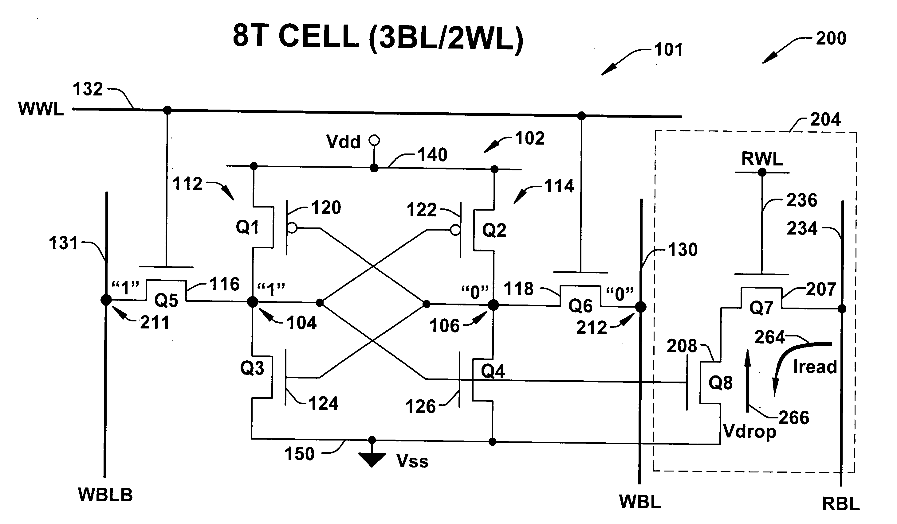
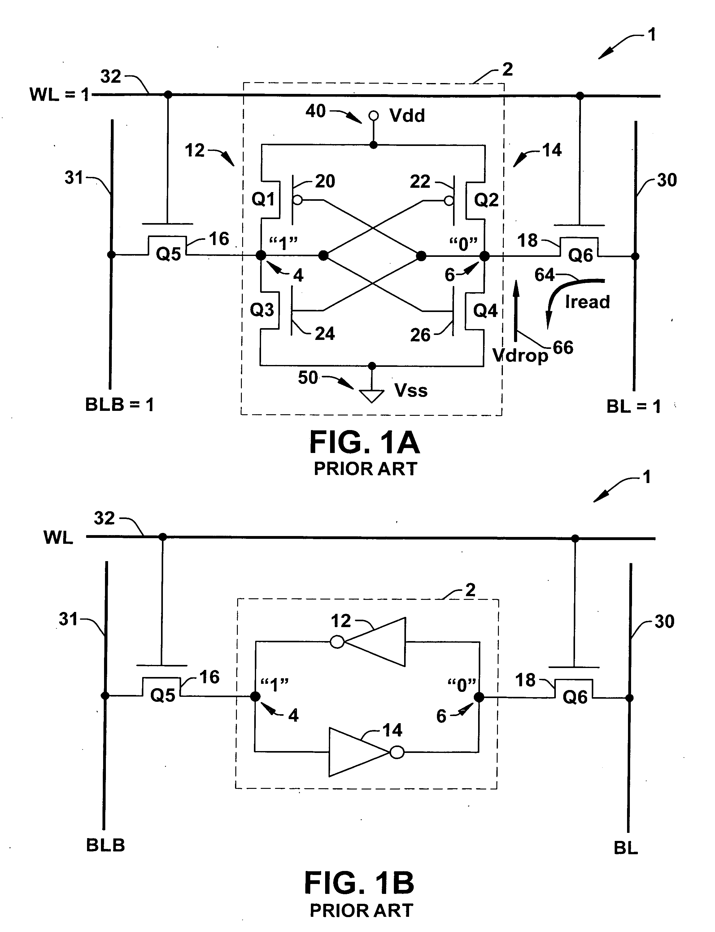
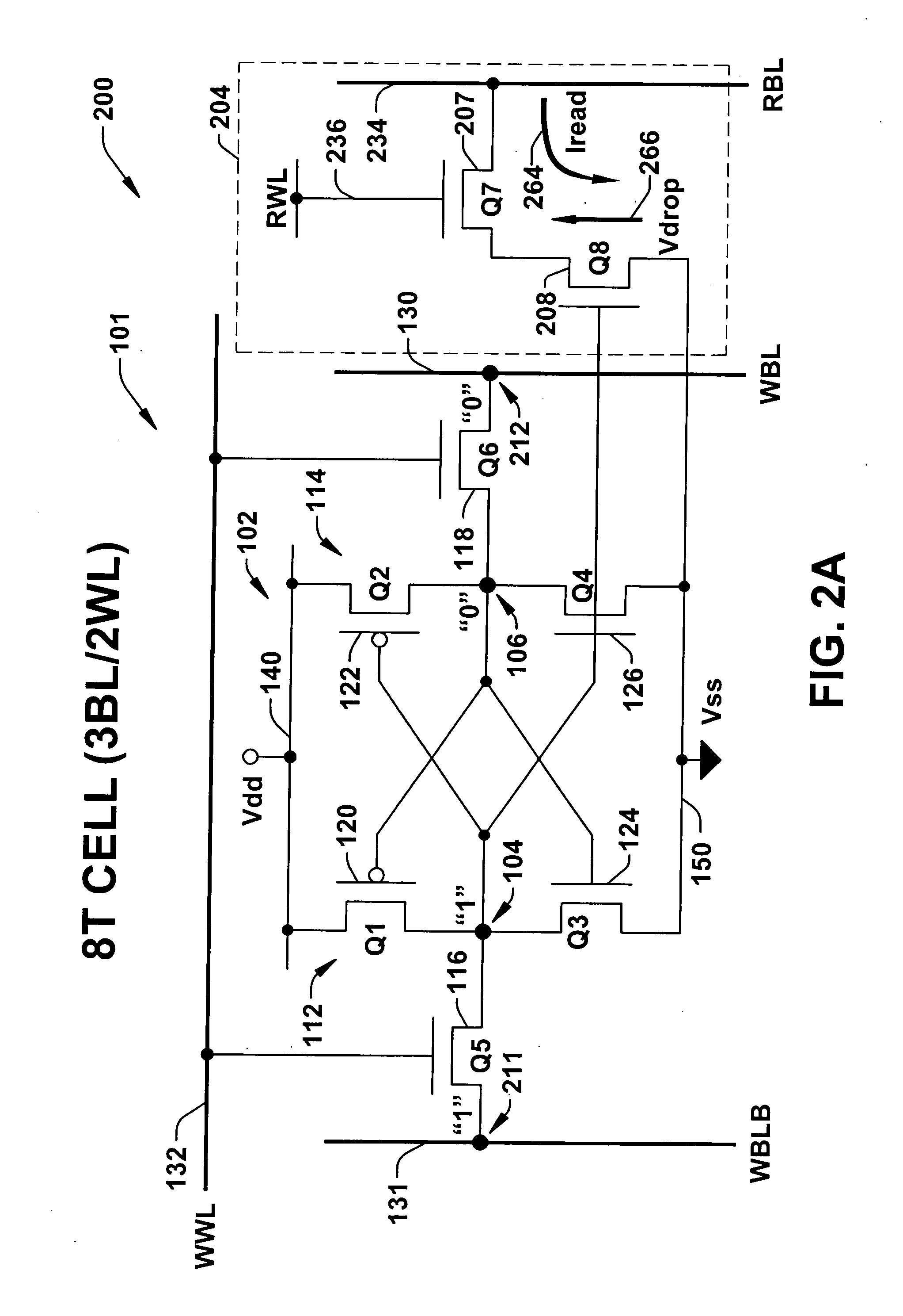
[0044]The present invention will now be described with reference to the attached drawings, wherein like reference numerals are used to refer to like elements throughout. The invention provides an SRAM memory cell structure (e.g., an 8T single ended and a 10T differential SRAM memory cell) utilizing a read buffer circuit for removing or isolating the read current from the latch nodes (data nodes) of the core cell or data cell during read operations, provides a separate read word line for selection of cell columns or a single cell during read operations, and provides a separate write word lines for selection of cell columns or a single cell during write operations.

[0045]Because the read current is isolated from the data storage cell of the present invention, the read drive current or maximum drive current through the read buffer may be increased over that which is often used in the write transistors of a conventional 6T differential cell. Further, the threshold voltage Vt used in the ...


PUM


Abstract

The present invention provides circuitry for writing to and reading from an SRAM cell core, an SRAM cell, and an SRAM device. In one aspect, the circuitry includes a write circuit coupled to the SRAM cell core that includes a write transistor gated by a write word line. The circuitry also includes a read buffer circuit coupled to the SRAM cell core to read the cell without disturbing the state of the cell. The read buffer circuit includes a read transistor gated by a read word line, the read transistor coupled between a read bit-line and a read driver transistor that is further coupled to a voltage source Vss. The read driver transistor and a first driver transistor of the cell core are both gated by one output of the cell core. The read transistor has an electrical characteristic that differs from that of the core cell first driver transistor.

Description

FIELD OF INVENTION[0001]The present invention relates generally to semiconductor memory devices, and more particularly to an improved stability SRAM memory cell having a read buffer circuit that permits a higher read voltage and current isolated from the latch nodes of the cell during read operations while permitting a lower write voltage that avoid upsets to the cell during write operations.BACKGROUND OF THE INVENTION[0002]Current trends in the semiconductor and electronics industry require memory devices to be made smaller, faster and require less power consumption. One reason for these trends is that more personal devices are being manufactured that are relatively small and portable, thereby relying on battery power. In addition to being smaller and more portable, personal devices are also requiring increased memory and more computational power and speed. In light of all these trends, there is an ever increasing demand in the industry for smaller, faster, and lower power dissipat...

Claims


Application Information

Patent Timeline
Patent Type & Authority Applications(United States)
IPC IPC(8): G11C11/00
CPCG11C11/412
Inventor HOUSTON, THEODORE WARREN
Owner TEXAS INSTR INC
Why Eureka
Try Eureka