
Memory system which copies successive pages, and data copy method therefor

a memory system and data copy technology, applied in the field of memory system and data copy method, can solve the problems of degrading data reliability, frequent copying of successive pages, repetitive page copying may generate many error bits which cannot be corrected by general error correction,

Active Publication Date: 2006-03-09
SOLID STATE SYST +1
View PDF4 Cites 49 Cited by
  • Summary
  • Abstract
  • Description
  • Claims
  • Application Information

AI Technical Summary

Benefits of technology

[0012] According to an aspect of the present invention, there is provided a memory system comprising a memory cell array in which electrically rewritable nonvolatile memory cells are arrayed, a first data buffer which holds, in read, data read from the memory cell array via a bit line switch and in write, data to be written in the memory cell array via the bit line switch, a second data buffer which is configured to swap data with the first data buffer, copies data to the first data buffer, and receives a copy of data from the first data buffer, a bus switch which is interposed between the second data buffer and a bus, selects part of data held by the second data buffer, and transfers the part of data to the b...

Problems solved by technology

This results in frequent copying of successive pages (page copy) in the NAND flash memory.
In this case, repetitive page copying may generate many error bits which cannot be corrected by general error correction in a read.
As described above, in the conventional memory system and the data copy method therefor, if no error correction is done in a read of a page subjected to page copying, repetitive page copying causes a data copy error, degrading the data reliability.
Error correction for preventing the degradation makes page copying very slow.

Method used


Image

  • Memory system which copies successive pages, and data copy method therefor
  • Memory system which copies successive pages, and data copy method therefor
  • Memory system which copies successive pages, and data copy method therefor

Examples


first embodiment

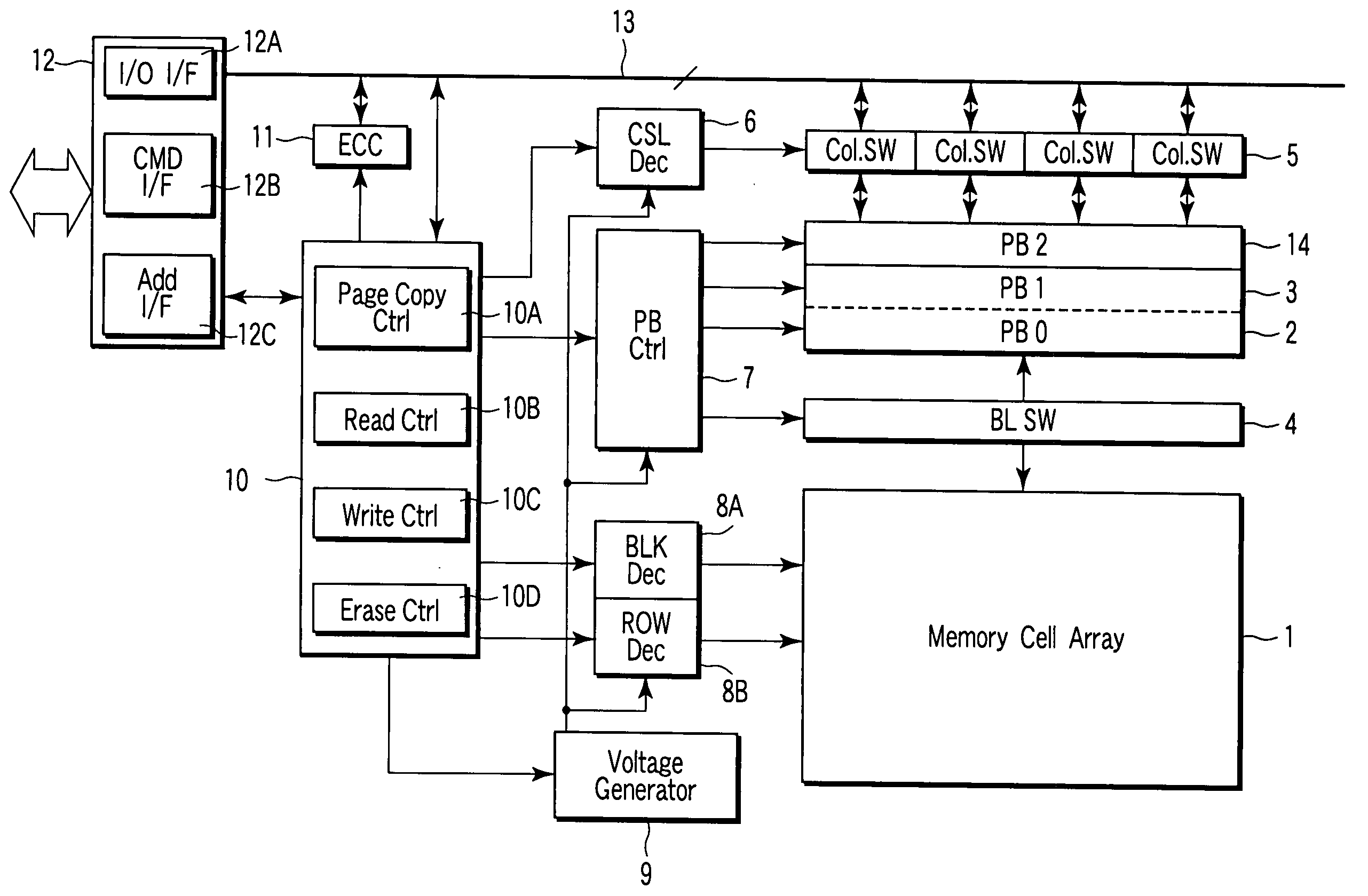
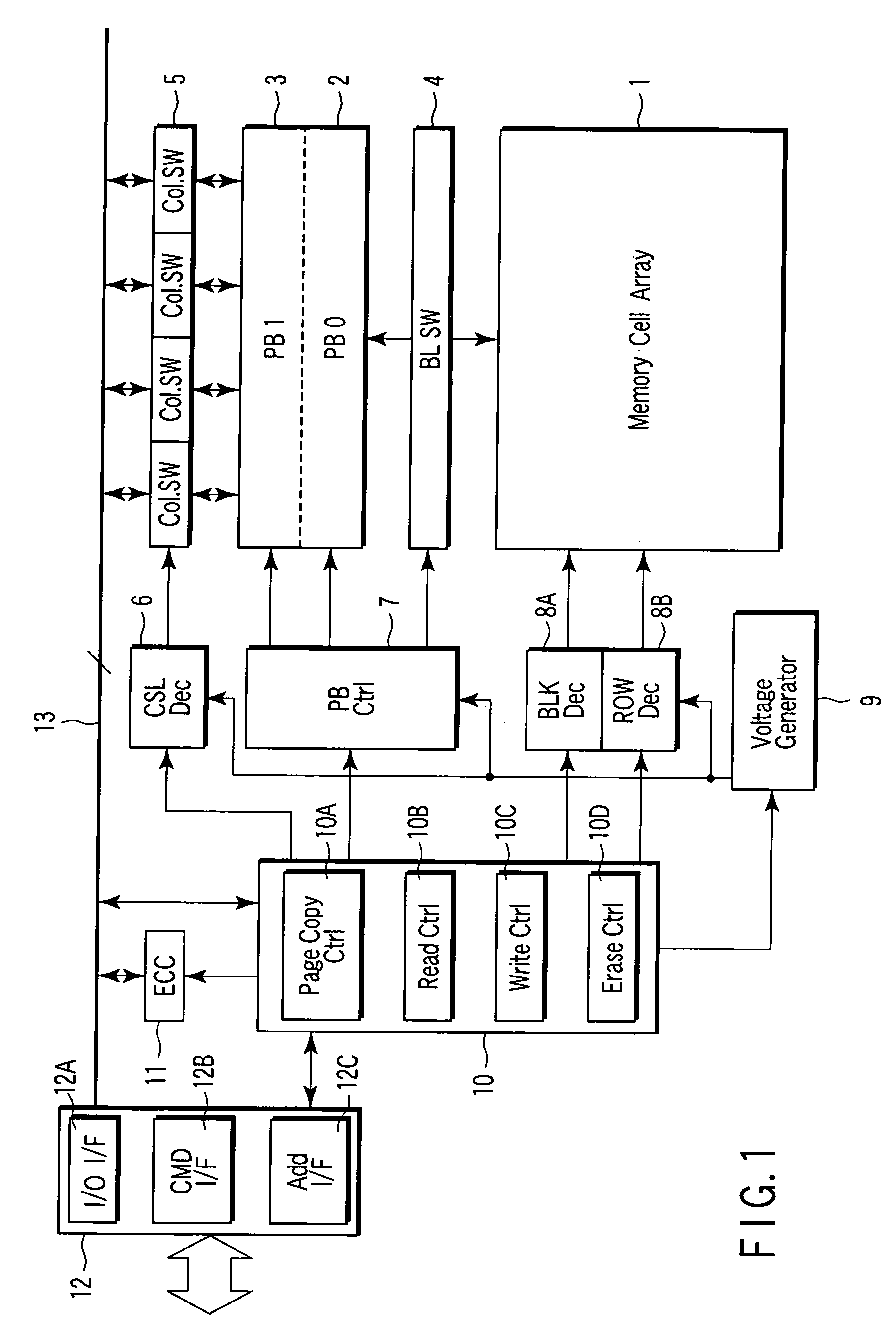
[0035]FIG. 1 is a block diagram showing the schematic arrangement of a NAND flash memory in order to explain a memory system and data copy method therefor according to the first embodiment of the present invention.

[0036] In a memory cell array 1, NAND strings are arrayed. The memory cell array 1 is connected to first and second page buffers (PB0 and PB1) 2 and 3 via a bit line switch (BL SW) 4. The first page buffer 2 comprises a functional unit serving as a sense amplifier and a functional unit serving as a data cache. The data cache holds sense data in read and write data in write. The page buffer 2 is so configured as to exchange data of each page with the second page buffer (PB1) 3. The page buffers 2 and 3 have a function of allowing their data to be copied to each other and swapping their data.

[0037] The page buffer 3 can input / output data by connecting a column designated by a CSL decoder (CSL Dec) 6 to an I / O bus 13 via a column switch (Col. SW) 5. When the bit width of th...

second embodiment

[0075]FIG. 10 is a flowchart showing a data copy method for a NAND flash memory in order to explain a memory system and data copy method therefor according to the second embodiment of the present invention. The second embodiment is directed to a case wherein copying is executed for each sector and the start and end positions of page copy are set in intermediate sectors.

[0076] A NAND flash memory generally reads and writes each page. In some cases, the start and end of page copy may be set not at the start of a page but midway in a page because the size of one page is large. For example, when the page size is 2 KB+64 B (64 B represents an area of an ECC code and management data) and the unit of data to be accessed is 512 B+16 B (to be referred to as a sector hereinafter), one page is made up of four sectors. The start of page copy may be the first page or the second (or third or fourth) sector, and the end of page copy may be the first (or second or third) sector.

[0077] In order to...

third embodiment

[0099]FIGS. 11 and 12 are views for explaining a memory system and data copy method therefor according to the third embodiment of the present invention. FIG. 11 is a block diagram showing the schematic arrangement of a NAND flash memory. FIG. 12 is a flowchart showing a copy sequence for a plurality of pages. Similar to the second embodiment, the third embodiment is directed to a case wherein copying is executed for each sector and reset sector data is externally complemented.

[0100] In the second embodiment, one page must be divided into sectors and repetitively rewritten by the sector. In this operation, the same word line is selected and written a plurality of number of times (equal to the number of sectors). The write stress (disturbance) is applied to the first written sector by “number of sectors−1” times, and the reliability of the memory cell degrades. Thus, write is desirably performed by the page. However, to perform data management of each sector by only write of each pag...


PUM


Abstract

A memory system includes a memory cell array, a bit line switch, first and second page buffers, a column switch, an error correction circuit, and control circuits. The second page buffer can swap data with the first page buffer. The control circuits controls the bit line switch and the first and second page buffers, sequentially reads, page by page, one or more pages from the mth (m is a positive integer) page to the nth (n is an integer greater than m) page of the first block in the memory cell array, controls the error correction circuit to perform error correction calculation by the error correction circuit, controls the first and second data buffers and the bit line switch, and controls to perform write in the second block in the erase state in the memory cell array.

Description

CROSS-REFERENCE TO RELATED APPLICATIONS [0001] This application is based upon and claims the benefit of priority from prior Japanese Patent Application No. 2004-257565, filed Sep. 3, 2004, the entire contents of which are incorporated herein by reference. BACKGROUND OF THE INVENTION [0002] 1. Field of the Invention [0003] The present invention relates to a memory system and data copy method therefor and, more particularly, to copying of successive pages in, e.g., a NAND flash memory, and is applied to system which performs error correction in copying. [0004] 2. Description of the Related Art [0005] In a NAND flash memory, as disclosed in, e.g., Jpn. Pat. Appln. KOKAI Publication No. 2002-141477, a memory cell has an n-channel MOSFET structure in which, for example, a floating gate and control gate are stacked as a charge storage multilayer. A plurality of memory cells of this structure are series-connected to each other so that adjacent memory cells share sources and drains. One NAN...

Claims


Application Information

Patent Timeline
IPC IPC(8): G06K15/00
CPCG11C16/0483G11C16/102G11C2216/14G11C2207/2236G11C16/26
Inventor SHIGA, HITOSHICHEN, CHIH-CHUNGWANG, CHIH-HUNGHUNG, SHENG-LIN
Owner SOLID STATE SYST
Learn More