
Multi-bit flash memory device including memory cells storing different numbers of bits

a flash memory and memory cell technology, applied in static storage, digital storage, instruments, etc., can solve the problems of affecting the operation of flash memory cells designed to store more bits, and affecting the operation of flash memory cells. , to achieve the effect of increasing the risk of programming and sensing errors, and reducing the number of bits

Active Publication Date: 2008-05-15
SAMSUNG ELECTRONICS CO LTD
View PDF6 Cites 50 Cited by
  • Summary
  • Abstract
  • Description
  • Claims
  • Application Information

AI Technical Summary

Benefits of technology

[0016]According to an embodiment of the present invention, a flash memory device comprises a memory cell array, a page buffer circuit, and a control logic unit. The memory cell array comprises first type memory cells capable of storing m-bit data and second type memory cells capable of storing n-bit data, where n is not equal to m. The page buffer circuit comprises a plurality of page buffers adapted to operate in programming, erasing, and reading operations of the first and second type memory cells. The control logic unit adapted to determine respective functions performed by the page buffers based on whether each page buffer is associated with first type memory cells or second type memory cells. Each page buffer comprises a plurality of latches adapted to store data for different purposes during programming and reading operations depending on the data storage capacities of corresponding memory cells among the first and second type memory cells.

Problems solved by technology

Volatile semiconductor memory devices often have higher operating frequencies than nonvolatile semiconductor memory devices, but they lose stored data when disconnected from an external power supply.
Unfortunately, however, it is relatively difficult to update stored data in MROMs, PROMs and EPROMs.
As a result, flash memory cells designed to store more bits tend to be more susceptible to programming and sensing errors.
Moreover, as variation occurs in processing conditions for forming the multi-bit cells, in voltage levels of selected word lines, in the operating voltage of the multi-bit cells, or the temperature of the multi-bit cells, it becomes more likely that sensing or programming errors will occur due to the small inter-threshold voltage distributions of multi-bit cells.
Unfortunately, page buffer technology for flash memory devices has not evolved to keep pace with the requirements of composite or multi-mode flash memory devices.
Unfortunately, this requirement for multiple page buffers tends to increase the chip size of flash memory devices.

Method used


Image

  • Multi-bit flash memory device including memory cells storing different numbers of bits
  • Multi-bit flash memory device including memory cells storing different numbers of bits
  • Multi-bit flash memory device including memory cells storing different numbers of bits

Examples


Embodiment Construction

[0035]Exemplary embodiments of the invention are described below with reference to the corresponding drawings. These embodiments are presented as teaching examples. The actual scope of the invention is defined by the claims that follow.

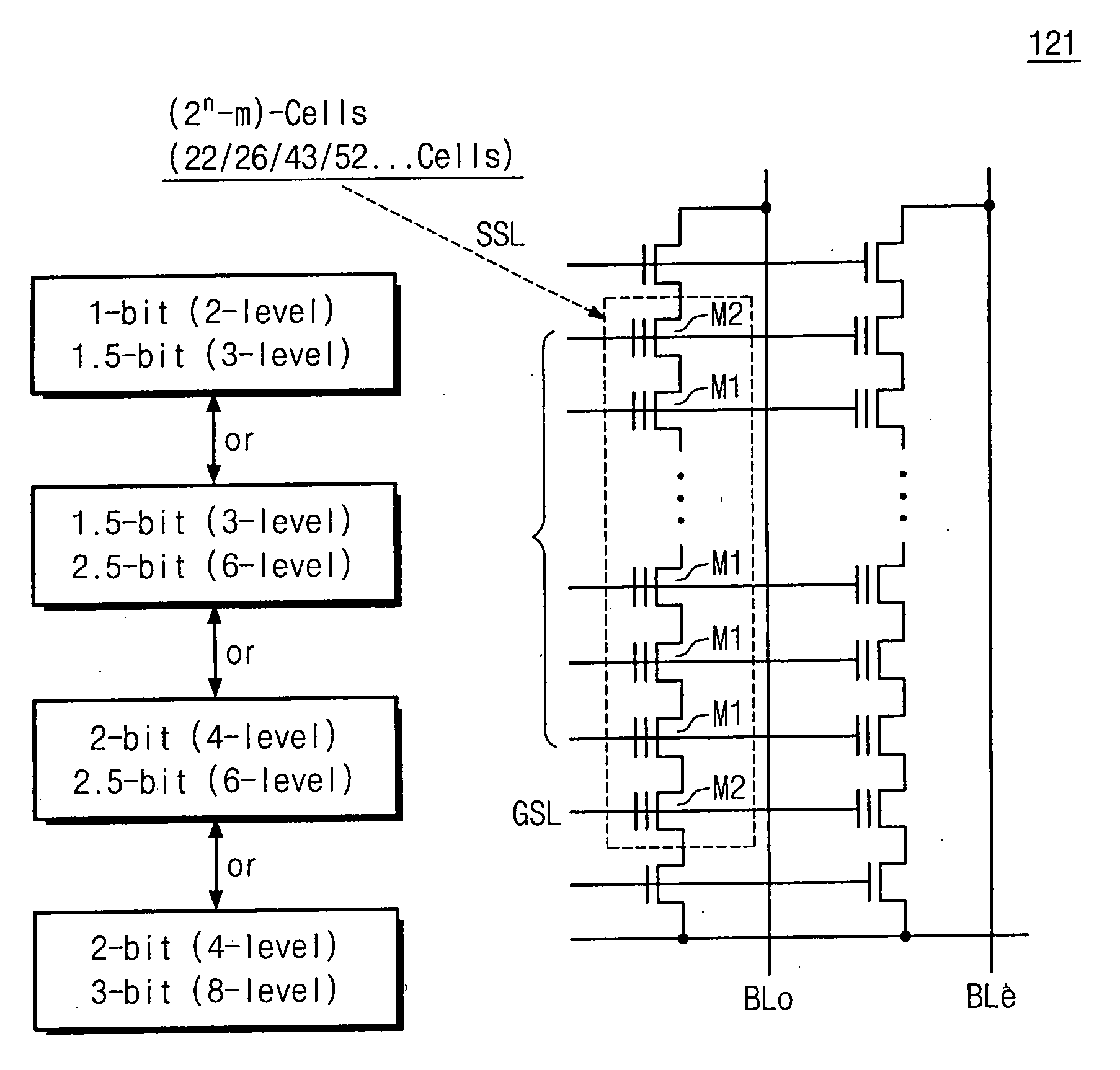
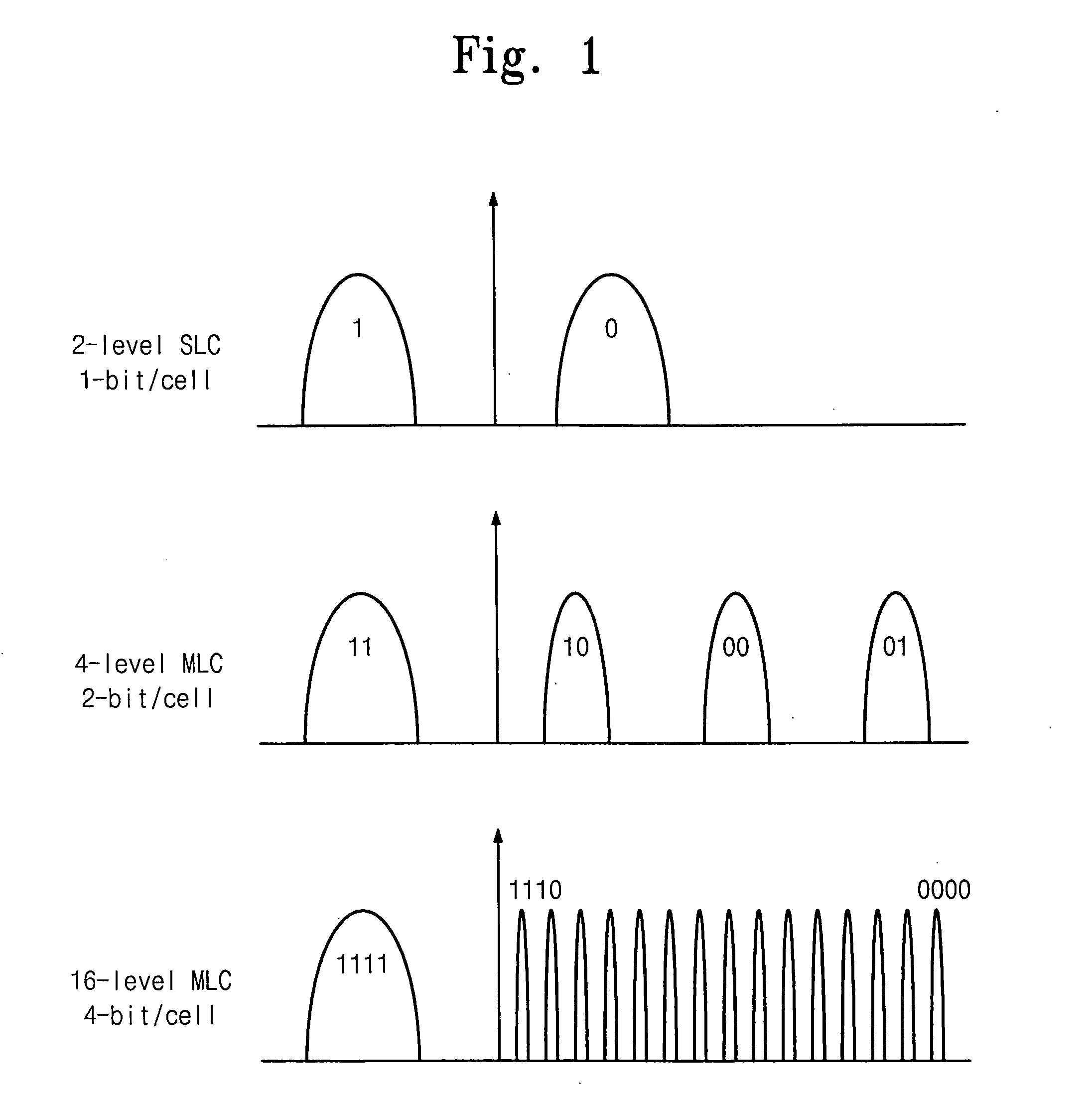
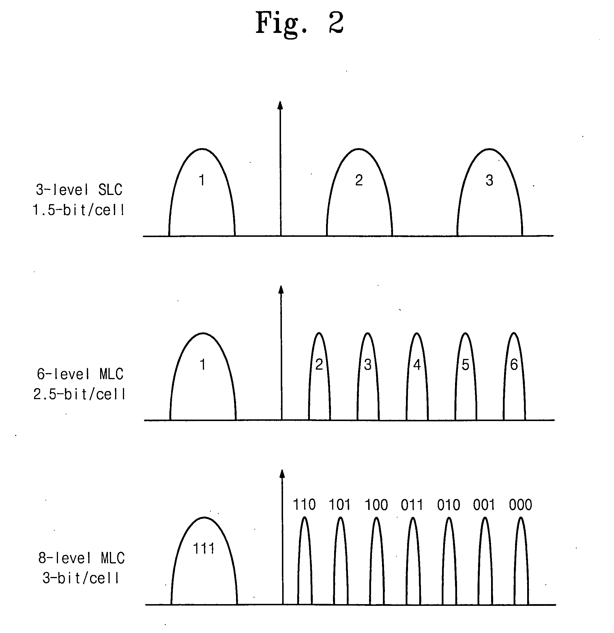
[0036]Data retention characteristics of memory cells included in flash memory devices according to selected embodiments of the invention can be established in various patterns according to user requirements. As an example, the data retention characteristics may be established by setting a state(s) of fuse(s) or by storing data in one or more registers. A control logic unit may then operate to control functions carried out by latches in page buffers of a page buffer circuit according to the data retention characteristics indicated by the state(s) of the fuse(s) or register(s). Thus, the device is able to conduct programming, reading, and erasing operations in selected memory cells without changing structures of the page buffers, even when the number of...


PUM


Abstract

A flash memory device comprises an array of memory cells capable of storing different numbers of bits per cell. A page buffer circuit for the flash memory device comprises a plurality of page buffers, each operating during programming, erasing, and reading operations of the memory cells. A control logic unit controls functions of the page buffers in accordance with the number of bits stored in corresponding memory cells.

Description

BACKGROUND OF THE INVENTION[0001]1. Field of the Invention[0002]Embodiments of the invention relate generally to semiconductor memory devices. More particularly, embodiments of the invention relate to multi-bit flash memory devices.[0003]A claim of priority is made to Korean Patent Application No. 2006-104611 filed on Oct. 26, 2006, the disclosure of which is hereby incorporated by reference in its entirety.[0004]2. Description of Related Art[0005]Semiconductor memory devices can be roughly divided into two categories: volatile and nonvolatile semiconductor memory devices. Volatile semiconductor memory devices often have higher operating frequencies than nonvolatile semiconductor memory devices, but they lose stored data when disconnected from an external power supply. On the other hand, nonvolatile memory devices tend to operate more slowly than volatile semiconductor memory devices, but can retain stored information even when disconnected from an external power supply. Due to this...

Claims


Application Information

Patent Timeline
IPC IPC(8): G11C14/00G11C16/04G11C11/34G11C7/10
CPCG11C11/5628G11C11/5642G11C16/0483G11C16/10G11C2211/5642G11C16/3454G11C2211/5621G11C2211/5641G11C16/12G11C16/04G11C16/06
Inventor PARK, KI-TAELEE, YEONG-TAEKKIM, KI-NAM
Owner SAMSUNG ELECTRONICS CO LTD
Learn More