Image sensor with 3D stack structure

a stack structure and image sensor technology, applied in the field of image sensors, can solve the problems of reducing resolution and overall resolution, and achieve the effect of avoiding resolution loss

Active Publication Date: 2015-02-26
SK HYNIX INC
View PDF3 Cites 13 Cited by
  • Summary
  • Abstract
  • Description
  • Claims
  • Application Information

AI Technical Summary

Benefits of technology

[0017]Preferably, a Talbot effect induction filter is provided at an upper portion of the first photodiode.
[0018]In accordance with an image sensor with a 3D stack structure according to the present invention, it is possible to realize a phase difference AF without loss of resolution.
[0019]Furthermore, as well as the realization of a phase difference AF function, it is possible to measure a distance between objects by modifying a structure of a bottom plate and to capture a three dimensional image.

Problems solved by technology

However, when the phase difference AF is realized on the sensor surface, since pixels to be used for forming an image are lost, overall resolution is reduced.
That is, in the structure of the conventional imaging surface phase difference AF, there is a problem that in order to improve resolution, it is difficult to realize the phase difference AF, and in order to realize precise phase difference AF, resolution is reduced.

Method used


Image

  • Image sensor with 3D stack structure
  • Image sensor with 3D stack structure
  • Image sensor with 3D stack structure

Examples


Embodiment Construction

[0029]Reference will now be made in greater detail to a preferred embodiment of the invention, an example of which is illustrated in the accompanying drawings. Wherever possible, the same reference numerals will be used throughout the drawings and the description to refer to the same or like parts.

[0030]The present invention is characterized in that in an image sensor with a 3D stack structure, different types of phase information generated when light having passed through a top plate is blocked by an artificial structure of a photodiode of a bottom plate is added to realize a phase difference AF.

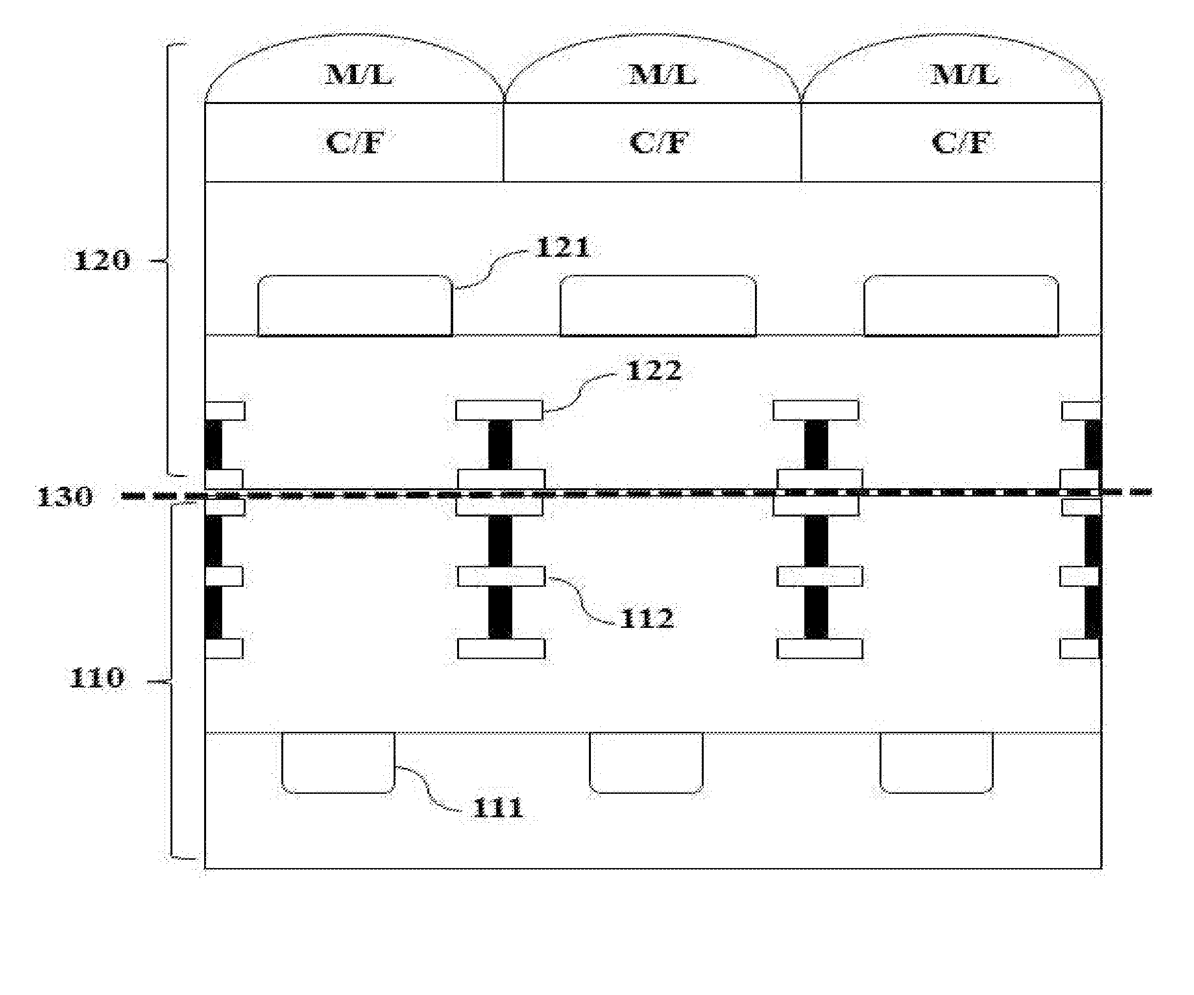
[0031]FIG. 1 is a diagram illustrating an embodiment of an image sensor with a 3D stack structure according to the present invention.

[0032]Referring to FIG. 1, the image sensor with a 3D stack structure has a stack structure of a first substrate 110 and a second substrate 120, wherein the first substrate 110 includes a first photodiode 111 and the second substrate 120 includes a second phot...


PUM


Abstract

Disclosed is an image sensor with a 3D stack structure, in which pixels of a top plate are realized as image pixels and pixels of a bottom plate are realized as pixels for realizing a phase difference AF, so that the phase difference AF is realized without loss of resolution. In the image sensor with a 3D stack structure, a problem of the reduction of resolution, which is a disadvantage of an existing imaging surface phase difference AF device, is solved, so that a fast phase difference AF is realized while maintaining high resolution without a separate phase difference AF module.

Description

BACKGROUND OF THE INVENTION[0001]1. Field of the Invention[0002]The present invention relates to an image sensor, and more particularly, to an image sensor with a 3D stack structure, in which pixels of a top plate are realized as image pixels and pixels of a bottom plate are realized as pixels for realizing a phase difference AF, so that the phase difference AF can be realized without loss of resolution.[0003]2. Description of the Related Art[0004]Recently, so-called electronic cameras are widely spread. The electronic camera operates through a process in which when an object is captured through an optical system, an image is formed on an image sensor that is a semiconductor imaging device, the image of the object is converted into an electrical signal, and image data of the obtained still image is recorded on a recording medium such as a semiconductor memory or a magnetic disk.[0005]Most electronic cameras are provided with an auto-focus (hereinafter, referred to as ‘AF’) device th...

Claims


Application Information

Patent Timeline
Patent Type & Authority Applications(United States)
IPC IPC(8): H01L27/146H04N13/02H04N5/232
CPCH01L27/14605H04N13/0214H04N5/23212H01L27/14629H01L27/14634H01L27/14647H01L27/1469H01L27/146
Inventor BYUN, KYUNG SU
Owner SK HYNIX INC
Why Eureka
Try Eureka