Semiconductor Component and Method of Triggering Avalanche Breakdown

a technology of electromagnetic discharge and component, applied in the direction of semiconductor devices, diodes, electrical apparatus, etc., can solve the problems of initiating current consumption and electrostatic discharg

Active Publication Date: 2015-03-12
INFINEON TECH AG
View PDF2 Cites 17 Cited by
  • Summary
  • Abstract
  • Description
  • Claims
  • Application Information

AI Technical Summary

Problems solved by technology

By way of example, avalanche breakdown typically initiates current consumption in electrostatic discharge (ESD) devices for protecting circuit blocks from damage by electrostatic discharge during assembly or operation.

Method used


Image

  • Semiconductor Component and Method of Triggering Avalanche Breakdown
  • Semiconductor Component and Method of Triggering Avalanche Breakdown
  • Semiconductor Component and Method of Triggering Avalanche Breakdown

Examples


Embodiment Construction

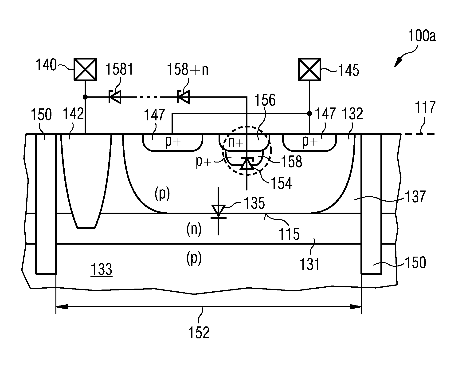
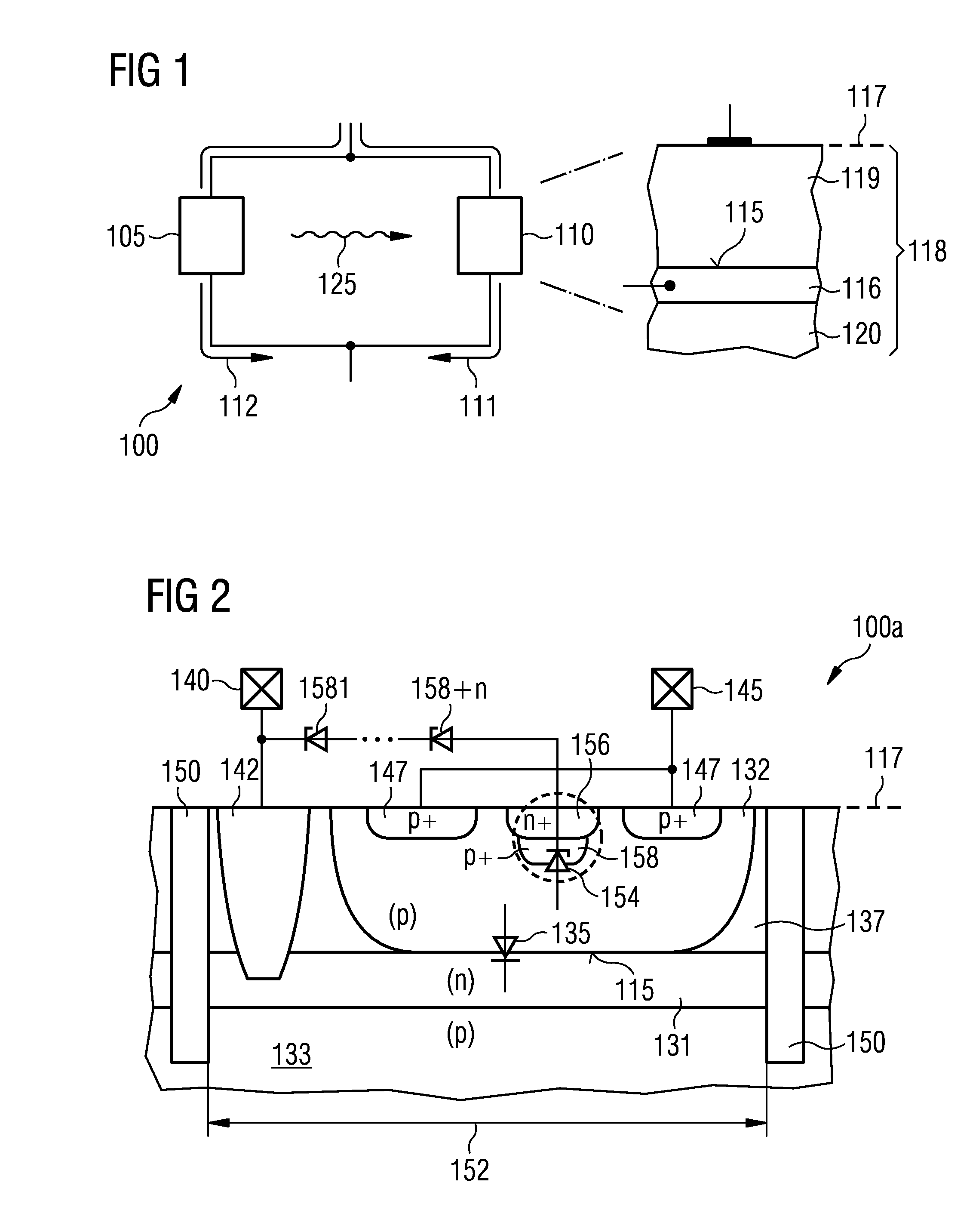
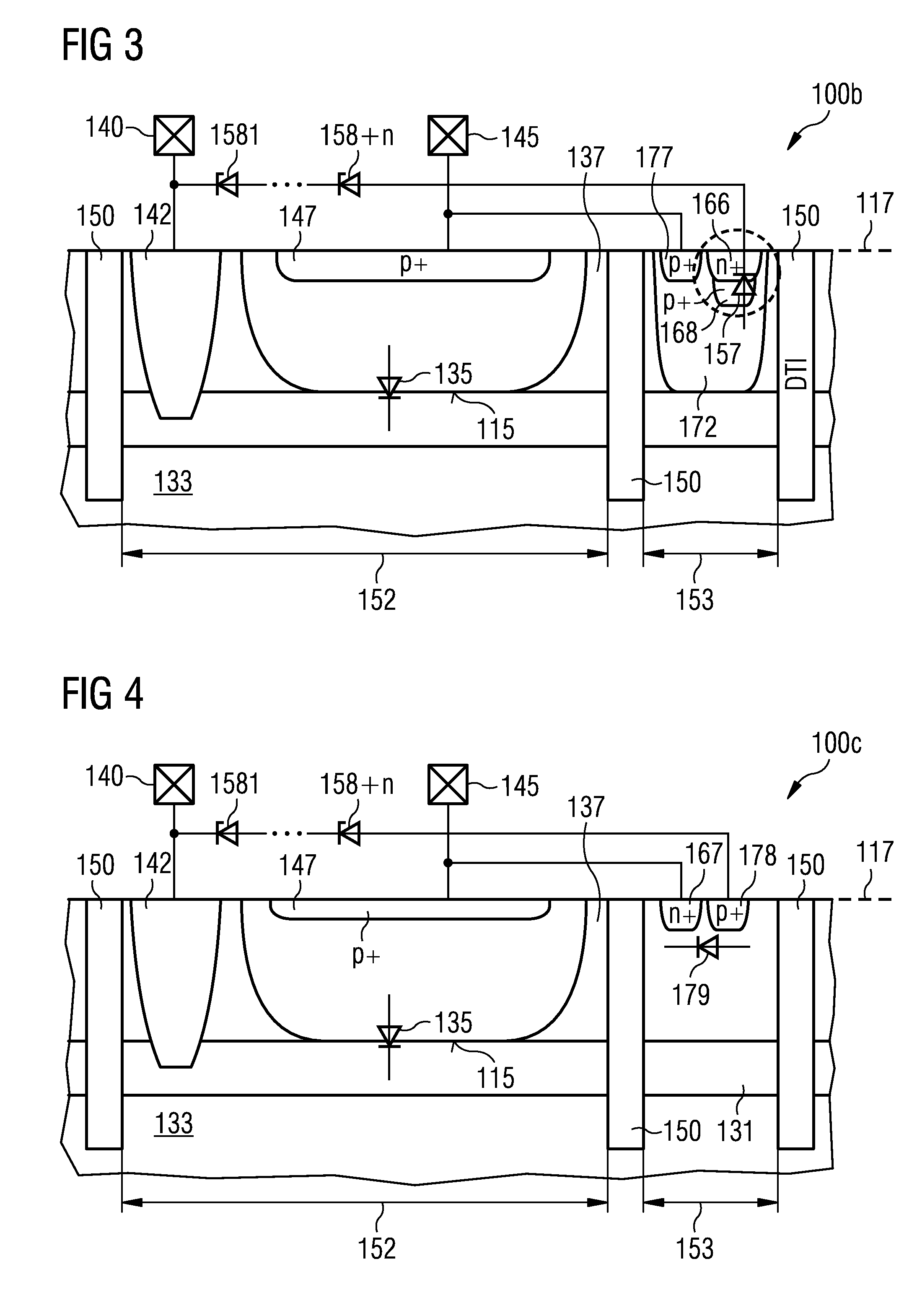
[0014]In the following detailed description, reference is made to the accompanying drawings, which form a part hereof, and in which are shown by way of illustrations specific embodiments in which the invention may be practiced. It is to be understood that other embodiments may be utilized and structural or logical changes may be made without departing from the scope of the present invention. For example, features illustrated or described for one embodiment can be used on or in conjunction with other embodiments to yield yet a further embodiment. It is intended that the present invention includes such modifications and variations. The examples are described using specific language that should not be construed as limiting the scope of the appending claims. The drawings are not scaled and are for illustrative purposes only. For clarity, the same elements have been designated by corresponding references in the different drawings if not stated otherwise.

[0015]The terms “having”, “contain...


PUM


Abstract

A semiconductor component includes an auxiliary semiconductor device configured to emit radiation. The semiconductor component further includes a semiconductor device. An electrical coupling and an optical coupling between the auxiliary semiconductor device and the semiconductor device are configured to trigger emission of radiation by the auxiliary semiconductor device and to trigger avalanche breakdown in the semiconductor device by absorption of the radiation in the semiconductor device. The semiconductor device includes a pn junction between a first layer of a first conductivity type buried below a surface of a semiconductor body and a doped semiconductor region of a second conductivity type disposed between the surface and the first layer.

Description

BACKGROUND[0001]Semiconductor components including semiconductor devices operating in avalanche breakdown mode are widespread in semiconductor applications. By way of example, avalanche breakdown typically initiates current consumption in electrostatic discharge (ESD) devices for protecting circuit blocks from damage by electrostatic discharge during assembly or operation.[0002]It is desirable to provide a semiconductor component having fast and reliable turn-on of avalanche breakdown and to provide a method of triggering avalanche breakdown in a semiconductor device.SUMMARY[0003]According to an embodiment of a semiconductor component, the semiconductor component includes an auxiliary semiconductor device configured to emit radiation. The semiconductor component further includes a semiconductor device. An electrical coupling and an optical coupling between the auxiliary semiconductor device and the semiconductor device are configured to trigger emission of radiation by the auxiliary...

Claims


Application Information

Patent Timeline
Patent Type & Authority Applications(United States)
IPC IPC(8): H01L31/173H01L27/02
CPCH01L27/0255H01L31/173H01L27/0629H01L27/15H01L29/808H02H3/20
Inventor WILLEMEN, JOOSTMAYERHOFER, MICHAELGLASER, ULRICHCAO, YIQUNMEISER, ANDREASHELL, MAGNUS-MARIASTECHER, MATTHIASLEBON, JULIEN
Owner INFINEON TECH AG
Why Eureka
Try Eureka