Method and structure for fabricating solar cells using a thick layer transfer process

a layer transfer and solar cell technology, applied in the direction of sustainable manufacturing/processing, nuclear engineering, final product manufacturing, etc., can solve the problems of low collection efficiency, many limitations of solar cells, and difficult manufacturing of materials, so as to increase collection efficiency

Inactive Publication Date: 2008-07-31
SILICON GENERAL CORPORATION
View PDF99 Cites 142 Cited by
  • Summary
  • Abstract
  • Description
  • Claims
  • Application Information

AI Technical Summary

Benefits of technology

[0011]In yet other alternatives according to embodiments of the present invention, the present method and structure provides one or more light trapping structures such as a plastic Fresnel sheet on the backside of the g

Problems solved by technology

Unfortunately, such petroleum sources have become depleted and have lead to other problems.
Although effective, these solar cells still have many limitations.
These materials are often difficult to manufacture.
Although these plates may be formed effectively, they do not possess optimum properties for highly effective solar cells.
Such single crystal silic

Method used


Image

  • Method and structure for fabricating solar cells using a thick layer transfer process
  • Method and structure for fabricating solar cells using a thick layer transfer process
  • Method and structure for fabricating solar cells using a thick layer transfer process

Examples


Embodiment Construction

[0030]According to embodiments of the present invention, techniques directed to the manufacture of photovoltaic materials are provided. More particularly, the invention provides a technique including a method and a structure for forming a solar cell structure using layer transfer techniques for photovoltaic applications. But it will be recognized that the invention has a wider range of applicability; it can also be applied to other types of applications such as for three-dimensional packaging of integrated semiconductor devices, photonic devices, piezoelectronic devices, flat panel displays, microelectromechanical systems (“MEMS”), nano-technology structures, sensors, actuators, integrated circuits, biological and biomedical devices, and the like.

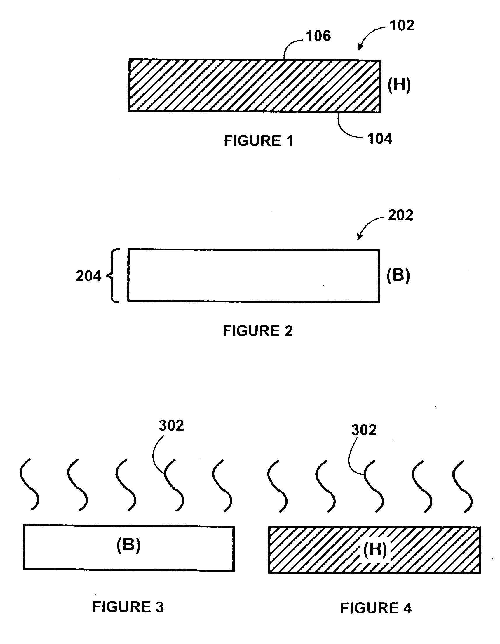
[0031]A method of manufacturing a photovoltaic layer on a semiconductor substrate is briefly outlined below.

[0032]1. Provide a semiconductor substrate, which has a surface region characterized by a tile configuration, a cleave region and a ...


PUM

PropertyMeasurementUnit
Thicknessaaaaaaaaaa
Thicknessaaaaaaaaaa
Thicknessaaaaaaaaaa

Abstract

A photovoltaic cell device, e.g., solar cell, solar panel, and method of manufacture. The device has an optically transparent substrate comprises a first surface and a second surface. A first thickness of material (e.g., semiconductor material, single crystal material) having a first surface region and a second surface region is included. In a preferred embodiment, the surface region is overlying the first surface of the optically transparent substrate. The device has an optical coupling material provided between the first surface region of the thickness of material and the first surface of the optically transparent material.

Description

CROSS-REFERENCES TO RELATED APPLICATIONS[0001]The instant nonprovisional application claims priority to U.S. Provisional Patent Application No. 60 / 825,095, filed Sep. 8, 2006 and incorporated by reference in its entirety herein for all purposes.BACKGROUND OF THE INVENTION[0002]Embodiments in accordance with the present invention relate generally to techniques including a method and a structure for forming a solar cell structure using layer transfer techniques for photovoltaic applications. But it will be recognized that the invention has a wider range of applicability; it can also be applied to other types of applications such as for three-dimensional packaging of integrated semiconductor devices, photonic devices, piezoelectronic devices, flat panel displays, microelectromechanical systems (“MEMS”), nano-technology structures, sensors, actuators, integrated circuits, biological and biomedical devices, and the like.[0003]From the beginning of time, human beings have relied upon the ...

Claims


Application Information

Patent Timeline
IPC IPC(8): H01L31/18H01L21/67G21K5/00
CPCH01L21/76254H01L31/03921H01L31/068Y10T29/41H01L31/1804Y02E10/544Y02E10/547H01L31/0687Y02P70/50H01L31/04H01L31/18
Inventor HENLEY, FRANCOIS J.
Owner SILICON GENERAL CORPORATION
Why Eureka
Try Eureka