Epitaxial substrate, semiconductor device, and method for manufacturing semiconductor device

a technology of semiconductor devices and substrates, which is applied in the direction of semiconductor devices, semiconductor/solid-state device details, electrical devices, etc., can solve the problem of not well studied the appropriate concentration of oxygen in silicon substrates

Inactive Publication Date: 2015-03-26
SANKEN ELECTRIC CO LTD +1
View PDF4 Cites 5 Cited by
  • Summary
  • Abstract
  • Description
  • Claims
  • Application Information

AI Technical Summary

Benefits of technology

[0008]An object of the present invention is to provide an epitaxial substrate, a semiconductor device, and a method for manufacturing the semiconductor device in which the occurrence of warpage caused by the stress between a silicon substrate and a semiconductor layer is suppressed by defining the concentrations of oxygen atoms and boron atoms which are contained in the silicon substrate.
[0012]According to the present invention, it is possible to provide an epitaxial substrate, a semiconductor device, and a method for manufacturing the semiconductor device in which the occurrence of warpage caused by the stress between a silicon substrate and a semiconductor layer is suppressed,.

Problems solved by technology

However, as for the silicon substrate to which boron has been added, an appropriate concentration of oxygen contained in the silicon substrate has not been well studied.

Method used


Image

  • Epitaxial substrate, semiconductor device, and method for manufacturing semiconductor device
  • Epitaxial substrate, semiconductor device, and method for manufacturing semiconductor device
  • Epitaxial substrate, semiconductor device, and method for manufacturing semiconductor device

Examples


Embodiment Construction

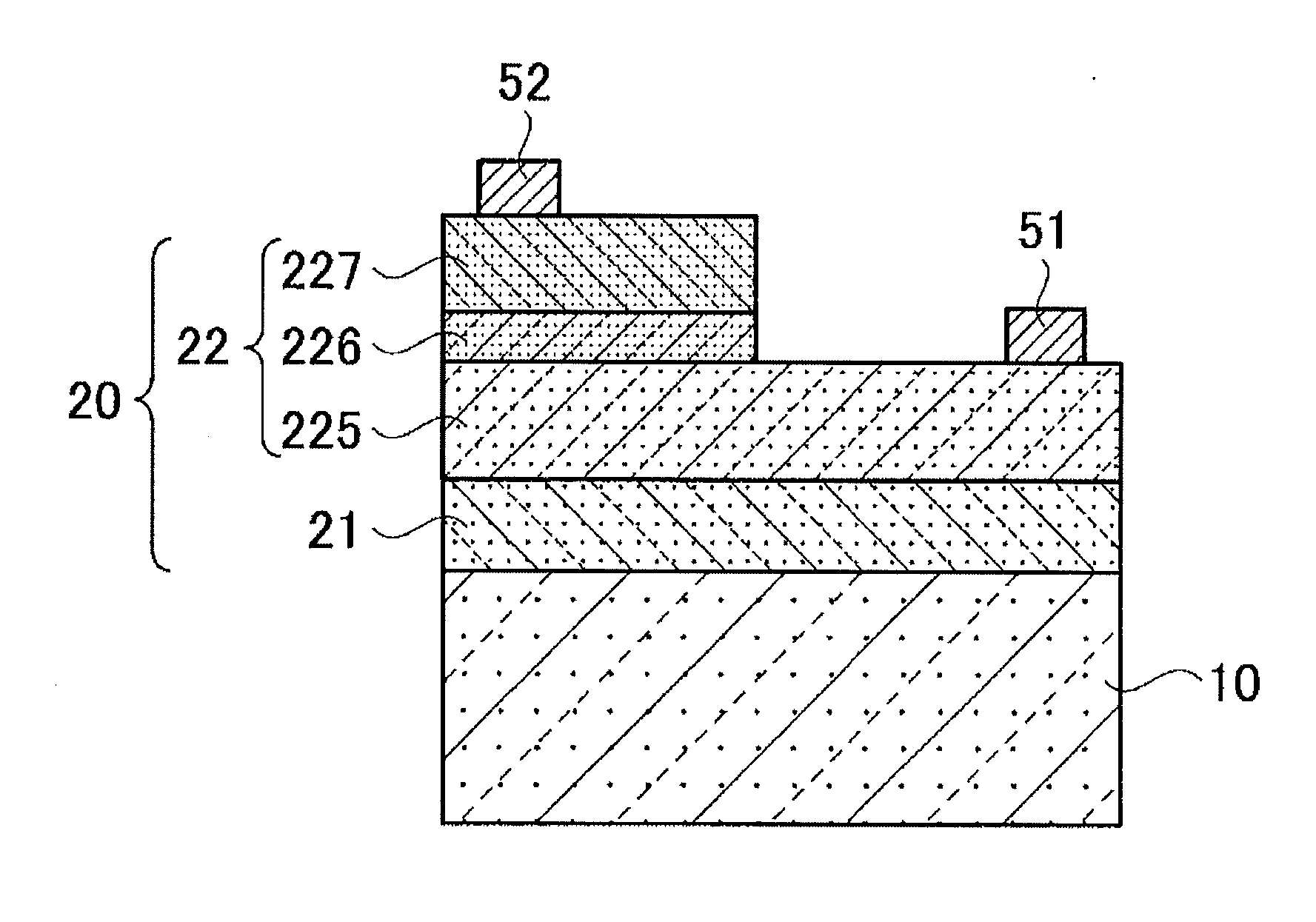
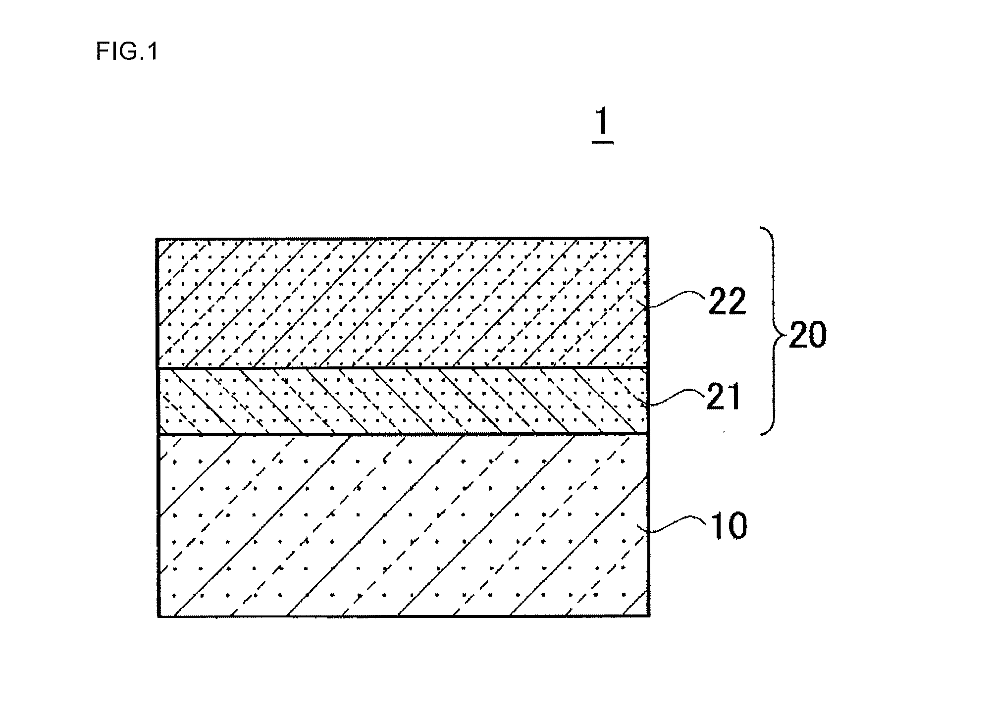
[0021]Next, with reference to the drawings, an embodiment of the present invention will be described. In the following descriptions of the drawings, the same or similar numerals are attached to the same or similar portions. However, it should be understood that the drawings are schematic drawings and the relationship between the thickness and the planar dimensions, the proportion of the length of each portion to the lengths of other portions, and so forth are different from the actual relationship and proportion. Therefore, specific dimensions have to be judged based on the following descriptions. Moreover, it goes without saying that the drawings also include a portion whose relationship and proportion of dimensions in one drawing differ from those in another drawing.

[0022]Moreover, the embodiment described below depicts an example of a device and a method for embodying the technical idea of this invention, and the technical idea of this invention does not limit the shapes, structu...


PUM

PropertyMeasurementUnit
temperatureaaaaaaaaaa
thicknessaaaaaaaaaa
thicknessaaaaaaaaaa

Abstract

The present invention provides an epitaxial substrate including a silicon substrate containing oxygen atoms in concentrations of 4×1017 cm−3 or more and 6×1017 cm−3 or less and containing boron atoms in concentrations of 5×1018 cm−3 or more and 6×1019 cm−3 or less and a semiconductor layer that is placed on the silicon substrate and is made of a material having a thermal expansion coefficient different from the thermal expansion coefficient of the silicon substrate. As a result, the epitaxial substrate in which the occurrence of warpage caused by the stress between the silicon substrate and the semiconductor layer is suppressed is provided.

Description

BACKGROUND OF THE INVENTION[0001]1. Field of the Invention[0002]The present invention relates to an epitaxial substrate having an epitaxially-grown layer formed on a silicon substrate, a semiconductor device, and a method for manufacturing the semiconductor device.[0003]2. Description of the Related Art[0004]In a semiconductor device, an epitaxial substrate having a semiconductor layer which is formed on an inexpensive silicon substrate by epitaxial growth and is made of a material, such as a nitride semiconductor, which is different from the material of the silicon substrate, is used. However, due to a difference in lattice constant and a difference in thermal expansion coefficient between the silicon substrate and the semiconductor layer, great stress is produced between the silicon substrate and the semiconductor layer at the time of epitaxial growth of the semiconductor layer or when the temperature is reduced. By generation of such great stress, plastic deformation appears in t...

Claims


Application Information

Patent Timeline
Patent Type & Authority Applications(United States)
IPC IPC(8): H01L23/00H01L29/20H01L21/02
CPCH01L23/562H01L21/02381H01L29/2003H01L21/02458H01L21/0254H01L21/02507H01L21/02521H01L21/0262H01L29/167H01L29/7786H01L33/007H01L2924/0002H01L29/872H01L2924/00
Inventor SHIKAUCHI, HIROSHIGOTO, HIROKAZUSATO, KENSHINOMIYA, MASARUTSUCHIYA, KEITAROHAGIMOTO, KAZUNORI
Owner SANKEN ELECTRIC CO LTD
Why Eureka
Try Eureka