Thin film transistor

a thin film transistor and transistor technology, applied in the direction of basic electric elements, electrical equipment, semiconductor devices, etc., can solve the problems of stress generation and electric properties may degrade, and achieve the effect of enhancing the stability of thin film transistors

Active Publication Date: 2010-01-19
AU OPTRONICS CORP
View PDF16 Cites 1 Cited by
  • Summary
  • Abstract
  • Description
  • Claims
  • Application Information

AI Technical Summary

Benefits of technology

[0009]In the present invention, a single-layer metal gate is replaced with a multi-layer metal gate comprising metals of capable of sustaining various levels and types of stress or Young's modulus, thus the stresses between the metal gate electrode and gate insulating layer can be reduced and the stability of thin film transistor can be enhanced. Moreover, in the described metal gate, each underlying metal layer has a Young's modulus less than that of the overlying ones.

Problems solved by technology

Stress is also generated by material defects.
Referring to FIG. 2, electric properties may degrade due to the existence of stresses between the metal gate electrode and gate insulating layer.

Method used


Image

  • Thin film transistor
  • Thin film transistor
  • Thin film transistor

Examples


Embodiment Construction

[0023]The following description is of the best-contemplated mode of carrying out the present invention. This description is made for the purpose of illustrating the general principles of the invention and should not be taken in a limiting sense. The scope of the invention is best determined by reference to the appended claims.

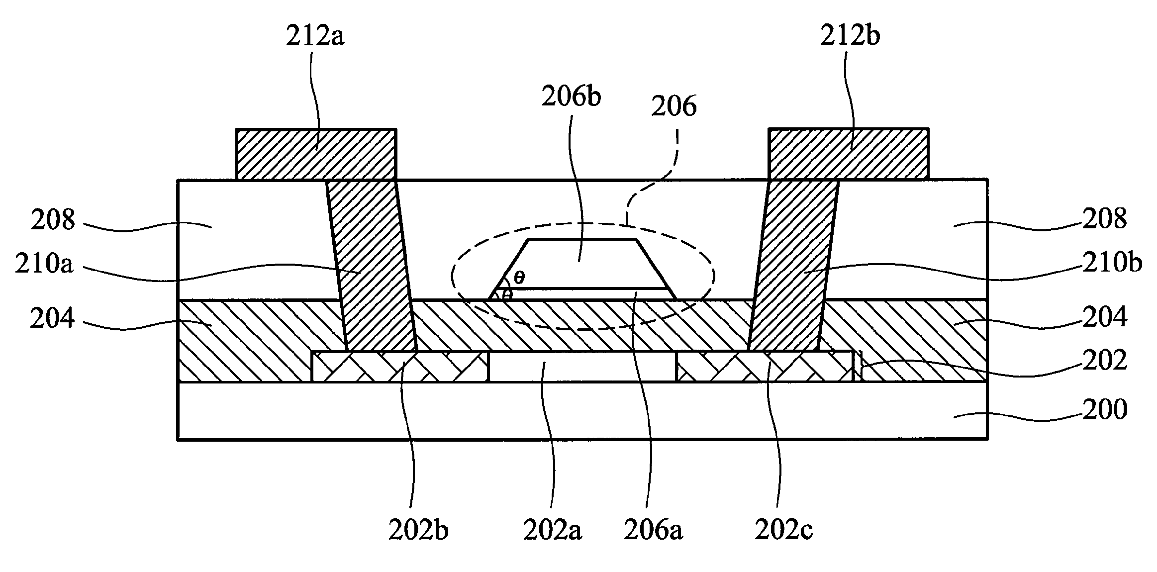
[0024]FIG. 3 shows an embodiment of a top gate type TFT comprising: a substrate 200; a polysilicon layer 202 on the substrate 200; a gate insulating layer 204 on the polysilicon layer 202; a gate electrode 206 on the gate insulating layer 204; an dielectric interlayer 208 on the gate electrode 206, and source and drain electrodes 212a and 212b electrically connected to the polysilicon layer 202 via plugs 210a and 210b, respectively. The polysilicon layer 202 only has three regions. The polysilicon layer 202 comprises a channel region 202a between the source region 202b, a drain region 202c. The gate electrode 206 is opposite to the channel region 202a against t...


PUM


Abstract

A thin film transistor is disclosed, comprising a substrate, a polysilicon layer overlying the substrate, a gate insulating layer overlying the polysilicon layer, a gate electrode, a dielectric interlayer overlying the gate electrode and gate insulating layer, and a source / drain electrode overlying the dielectric interlayer. Specifically, the gate electrode comprises a first electrode layer overlying the gate insulating layer and a second electrode layer essentially overlying an upper surface of the first electrode layer. The first and second electrode layers each has substantially the same profile with a taper angle of less than about 90 degrees.

Description

BACKGROUND OF THE INVENTION[0001]1. Field of the Invention[0002]The invention relates to a thin film transistor, and more particularly to a thin film transistor (TFT) for a low temperature polysilicon (LTPS) display.[0003]2. Description of the Related Art[0004]As shown in FIG. 1, a conventional top gate type TFT comprises a substrate 100, a polysilicon layer 102 on the substrate 100, a gate insulating layer 104 on the polysilicon layer 102, a gate electrode 106 on the gate insulating layer 104, an dielectric interlayer 108 on the gate electrode 106, and source and drain electrodes 112a, 112b electrically connected to the source and drain regions 102b and 102c of the polysilicon layer 102 by means of the plugs 110a and 110b, respectively. The gate electrode 106 may include Mo or W. Stress is typically generated during deposition of films and thermal processes and remains in or between films, e.g. between the gate electrode and gate insulating layer. Stress is also generated by materi...

Claims


Application Information

Patent Timeline
Patent Type & Authority Patents(United States)
IPC IPC(8): H01L27/14H01L29/04H01L29/15H01L31/036
CPCH01L29/42384H01L29/4908
Inventor CHANG, CHIH-HSIUNGWENG, CHIEN-SHENHSU, CHIEH-CHOUPENG, CHIA-TIENLI, JHEN-YUE
Owner AU OPTRONICS CORP
Why Eureka
Try Eureka