
Touch panel
a capacitive touch panel and projecting technology, applied in the field of touch panels, can solve the problems of increasing the difficulty of subsequent steps for layer disposition and film patterning, affecting the quality of the touch panel, and affecting the signal attenuation or triggering of the electrostatic discharge effect, so as to improve the ability to resist the static discharge effect
- Summary
- Abstract
- Description
- Claims
- Application Information
AI Technical Summary
Benefits of technology
Problems solved by technology
Method used
Image

Examples
Embodiment Construction
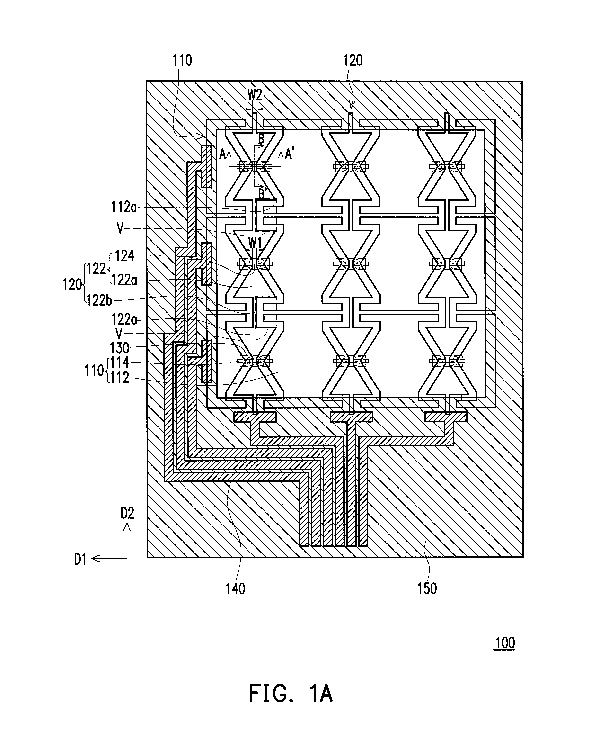
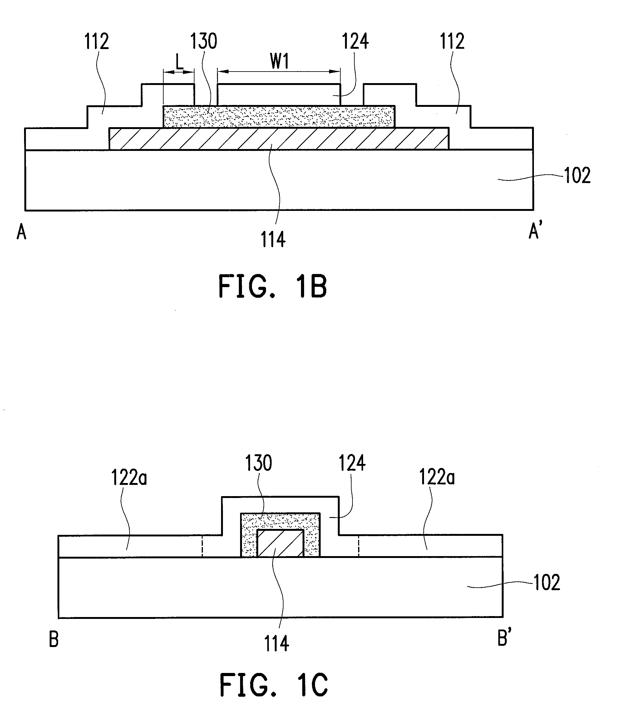
[0048]FIG. 1A is a schematic top view of a touch panel according to an embodiment of the invention. FIG. 1B is a schematic cross-sectional view taken along line A-A′ depicted in FIG. 1A. FIG. 1C is a schematic cross-sectional view taken along line B-B′ depicted in FIG. 1A. Referring to FIG. 1A, FIG. 1B and FIG. 1C, a touch panel 100 includes a substrate 102, a plurality of first conductive elements 110, a plurality of second conductive elements 120, a plurality of insulation patterns 130, a plurality of signal transmission lines 140 and a decoration layer 150. The touch panel 100 may include a light transmissive region and a light shielding region for being positioned on or integrated with a display. The light transmissive region corresponds to display units such as a liquid crystal display or an organic light-emitting diode, and the light shielding region is configured to shade visible elements or light not intended to be seen, such element may be, for example, the signal transmiss...
PUM
 Abstract
Description
Claims
Application Information