Substrate inspection apparatus

a technology of substrate and inspection apparatus, which is applied in the direction of measurement devices, semiconductor/solid-state device testing/measurement, instruments, etc., can solve the problems of excessive contact between devices and electrodes, and the number of electrodes can be reduced, so as to suppress the strong contact and reduce the decompression range of sealed space

Inactive Publication Date: 2015-05-14
TOKYO ELECTRON LTD
View PDF7 Cites 10 Cited by
  • Summary
  • Abstract
  • Description
  • Claims
  • Application Information

AI Technical Summary

Benefits of technology

[0016]In accordance with the example embodiments, the decompressing device configured to decompress the sealed space between the substrate and the probe card includes the suction opening; the decompression chamber communicating with the suction opening; the exhaust opening communicating with the decompression chamber; and the discharge opening configured to discharge a fluid toward the decompression chamber at a high velocity. Since the discharge opening and the exhaust opening are formed to directly confront with each other, the high-velocity fluid draws a gas within the decompression chamber, and then, the drawn gas is exhausted through the exhaust opening. As a result, a negative pressure is generated in the decompression chamber and, also, in the suction opening communicating with the decompression chamber. The amount of the gas drawn from the decompression chamber is smaller than the amount of the high-velocity fluid discharged from the discharge opening. Accordingly, even if the amount of the high-velocity fluid discharged from the discharge opening is greatly varied, the amount of the gas drawn from the decompression chamber is still small. Since there is a correlation between the amount of the gas drawn from the decompression chamber and the variation range of the negative pressure in the suction opening, the control range of the negative pressure in the suction opening can be reduced, so that the decompression range of the sealed space can also be reduced. As a consequence, it is possible to suppress the strong contact between each probe and each corresponding electrode of each semiconductor device. Accordingly, when inspecting electrical characteristics of each semiconductor device on the substrate, deep needle marks may not be left on each electrode of each semiconductor device on the substrate, and the probe or the substrate can be suppressed from being damaged.

Problems solved by technology

Since, however, a contact surface formed by leading ends of the individual probes and a mounting surface of the stage on which the wafer is mounted are not always parallel to each other, a part of the multiple number of probes and a part of a multiple number of electrodes of the semiconductor devices may be brought into excessively strong contact with each other, whereas another part of the multiple number of probes and another part of the electrodes may not be brought into contact with each other at all.
That is, all the probes may not be brought into contact with the corresponding electrodes of the semiconductor devices in a uniform manner.

Method used


Image

  • Substrate inspection apparatus
  • Substrate inspection apparatus
  • Substrate inspection apparatus

Examples


Embodiment Construction

[0020]Hereinafter, example embodiments will be explained with reference to the accompanying drawings, which form a part hereof.

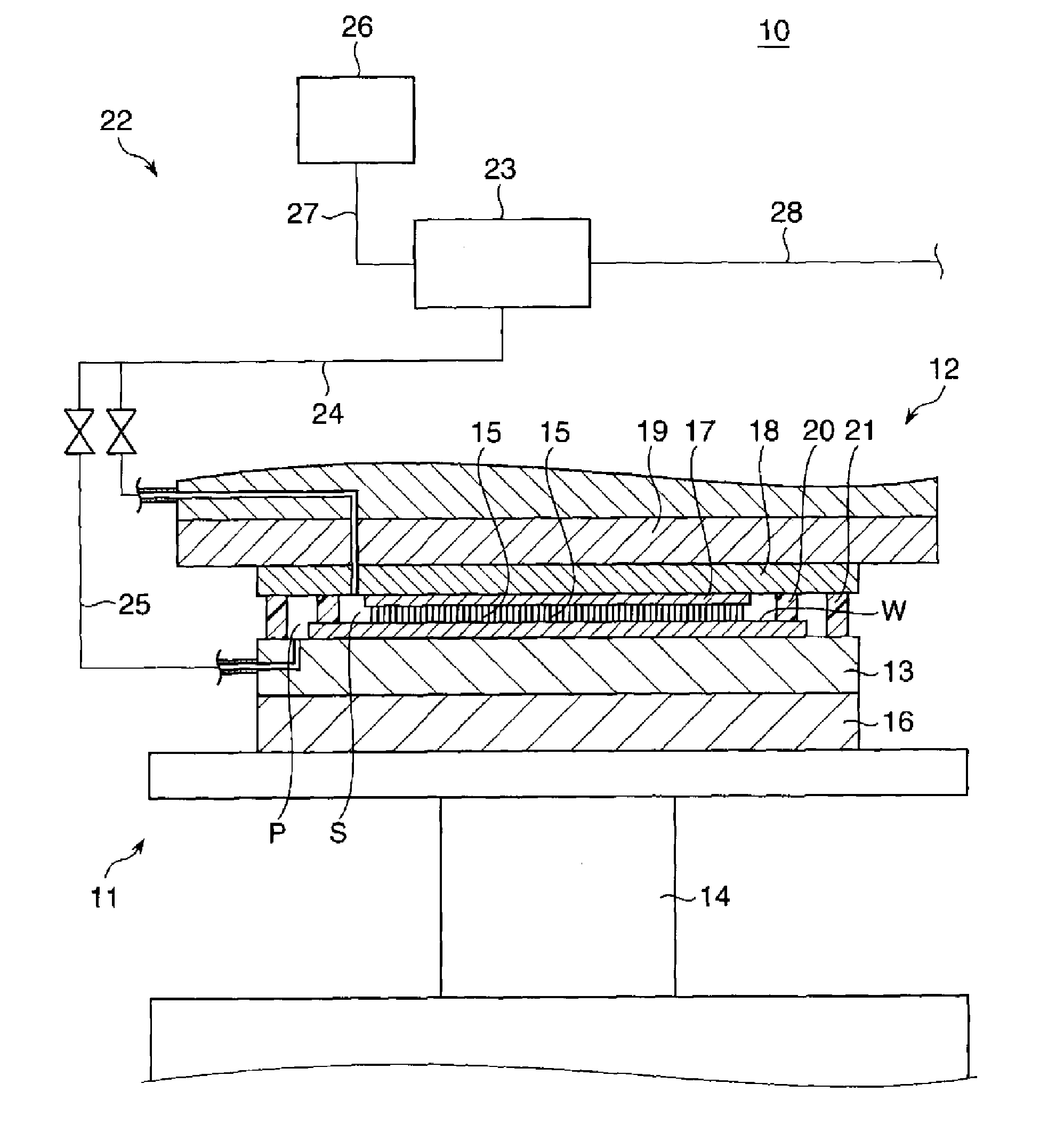
[0021]FIG. 1 is a cross sectional view schematically illustrating a configuration of a substrate inspection apparatus in accordance with an example embodiment.

[0022]In FIG. 1, a probe apparatus 10 serving as a substrate inspection apparatus includes a stage 11 configured to mount thereon a wafer W to be inspected; and an inspection unit 12 provided to face the stage 11.

[0023]The stage 11 includes a wafer plate 13 made of a plate-shaped member configured to mount thereon the wafer W (substrate) directly; a shaft 14 configured to move the wafer plate 13 in a vertical direction of the drawing; and a plate-shaped chuck member 16 provided on a leading end of the shaft 14 and configured to attract the wafer plate 13.

[0024]The inspection unit 12 includes a probe card 17 placed to face the wafer W mounted on the wafer plate 13; a contact plate 18 made of a plate-sha...


PUM


Abstract

A probe apparatus 10 that maintains a contact state between each of probes 15 of a probe card 17 and each of corresponding electrodes of semiconductor devices formed on a wafer W by maintaining a decompressed state of a sealed space S between the wafer W and the probe card 17 includes an ejector 23 configured to decompress the sealed space S. Further, the ejector 23 includes a suction port 29; a decompression chamber 31 communicating with the suction port 29; an exhaust port 34 communicating with the decompression chamber 31; and a nozzle 32 through which air is discharged toward the decompression chamber 31 at a high velocity. Furthermore, the nozzle 32 is configured to directly confront the exhaust port 34, and the suction port 29 communicates with the sealed space S.

Description

TECHNICAL FIELD[0001]The embodiments described herein pertain generally to a substrate inspection apparatus having a probe card.BACKGROUND[0002]As a substrate inspection apparatus, for example, there is known a probe apparatus that inspects electrical characteristics of a multiple number of semiconductor devices formed on a wafer as a substrate.[0003]Typically, the probe apparatus includes a stage that can be moved in X, Y, Z and θ directions while mounting the wafer thereon; a head plate provided above the stage; and a probe card provided to the head plate to face the stage. The probe card has a multiple number of probes (inspection needles) protruding toward the stage.[0004]In this probe apparatus, alignment (position adjustment) between the probes of the probe card and corresponding electrodes of the semiconductor devices formed on the wafer is performed by moving the stage relatively with respect to the head plate. Then, by moving the stage upward, each probe of the probe card a...

Claims


Application Information

Patent Timeline
Patent Type & Authority Applications(United States)
IPC IPC(8): G01R31/28G01R1/067
CPCG01R1/06705G01R31/2891G01R31/28G01R31/2851H01L22/30H01L22/34G01R1/07314G01R31/2887
Inventor YAMADA, HIROSHI
Owner TOKYO ELECTRON LTD
Why Eureka
Try Eureka