

Liquid crystal display panel
- Summary
- Abstract
- Description
- Claims
- Application Information
AI Technical Summary
Benefits of technology
Problems solved by technology
Method used
Image

Examples
Embodiment Construction
[0034]The present disclosure will be introduced in detail below with reference to the accompanying drawings.
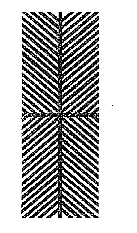
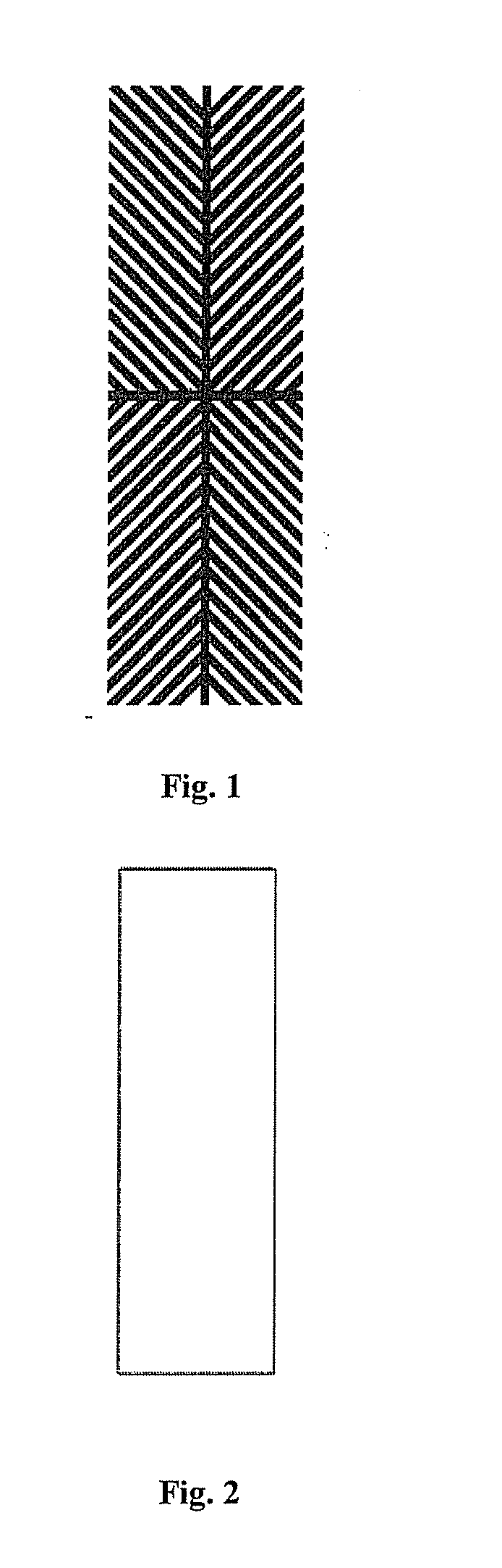
[0035]FIG. 4 schematically shows the structure of a pixel electrode of a thin-film transistor (TFT) array substrate of a liquid crystal display panel according to the present disclosure. The pixel electrode is arranged on one side of a liquid crystal layer where a TFT is arranged, and is used for the array substrate. The pixel electrode of the TFT array substrate is formed in a “fishbone” shape. Namely, the whole electrode is divided into a plurality of display areas through strip-like trunk electrode portions that are vertically crossed with each other, and in each of the display areas strip-like branch electrodes that are mutually separated from each other are arranged.
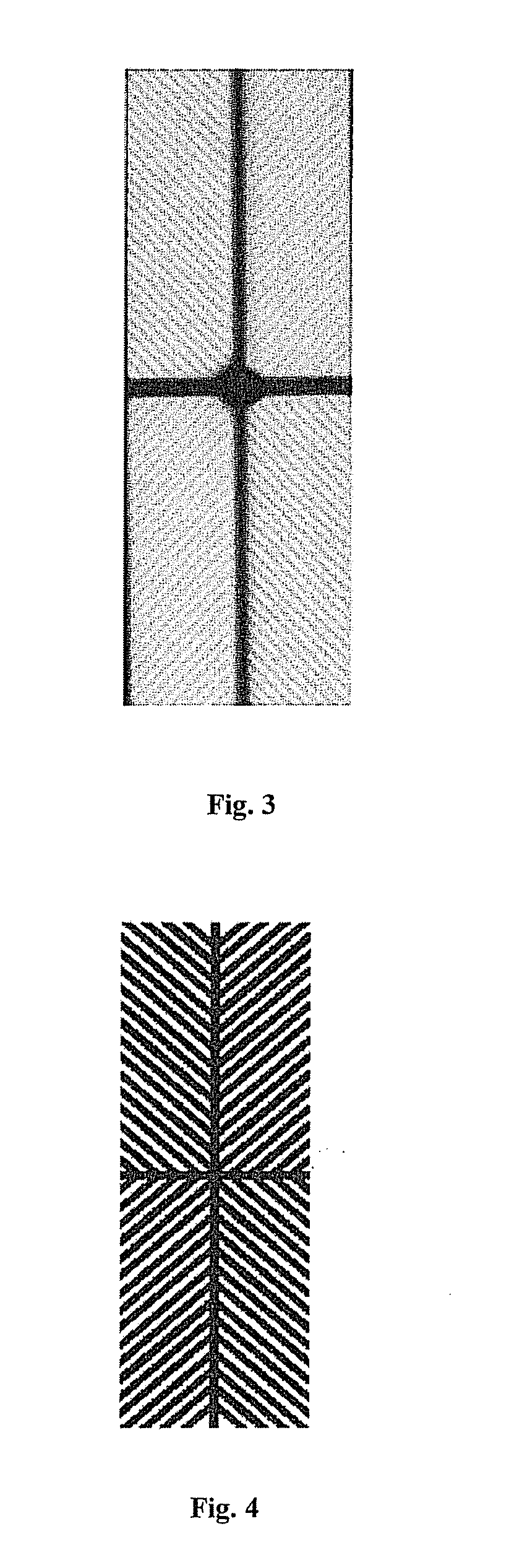
[0036]FIG. 5 schematically shows the structure of a common electrode of a color filter (CF) substrate of the liquid crystal display panel according to the present disclosure. The common electrode is arranged o...
PUM
 Abstract
Description
Claims
Application Information