Semiconductor element drive device

a technology of magnetic drive and element, which is applied in the direction of emergency protective arrangements for limiting excess voltage/current, instruments, pulse techniques, etc., can solve the problems of difficult to distinguish between alarm signals, inability to detect anomaly cancellation, and long time until anomaly cancellation is detected, so as to facilitate and quickly detect the cancellation of anomaly factors, accurately distinguish the type of anomalies, and detect the effect of anomaly cancellation

Active Publication Date: 2015-06-25
FUJI ELECTRIC CO LTD
View PDF4 Cites 14 Cited by
  • Summary
  • Abstract
  • Description
  • Claims
  • Application Information

AI Technical Summary

Benefits of technology

[0015]According to the semiconductor element drive device of this kind of configuration, one pulse's worth of alarm signal with a pulse width corresponding to an anomaly factor occurring in a semiconductor element is output, or one pulse's worth of alarm signal is output after every preset time interval. Consequently, it is easy to detect the pulse width of an alarm signal notified from the drive device, and it is possible to accurately distinguish the type of an anomaly based on the pulse width of the detected alarm signal. Moreover, a protection cancellation signal of a level differing from that of the alarm signal is output when the anomaly factor of the semiconductor element is cancelled and the output of the alarm signal finishes. Consequently, even without detecting the pulse width of the protection cancellation signal,

Problems solved by technology

However, when a plurality of alarm signals with different pulse widths are output from the notification circuit at the same time, there is included the problem of it being difficult to distinguish between the alarm signals.
However, when an anomaly of a semiconductor element is detected, it is only that one pulse's worth of alarm signal with a pulse width corresponding to the type of the anomaly is output, or that one pulse's worth of alarm signal is output after every preset

Method used


Image

  • Semiconductor element drive device
  • Semiconductor element drive device
  • Semiconductor element drive device

Examples


Embodiment Construction

[0022]Hereafter, a description will be given, referring to the drawings, of embodiments of the invention.

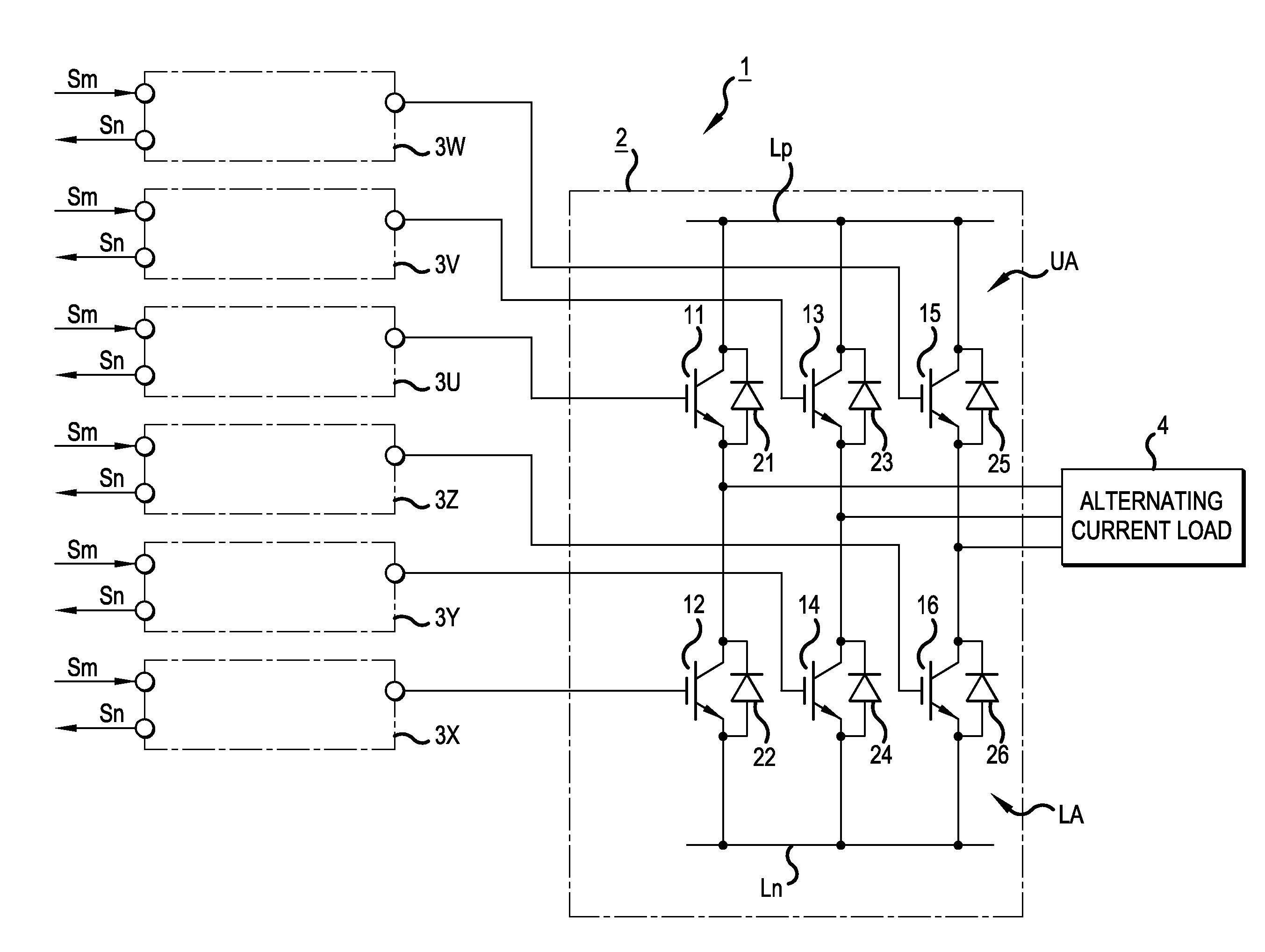
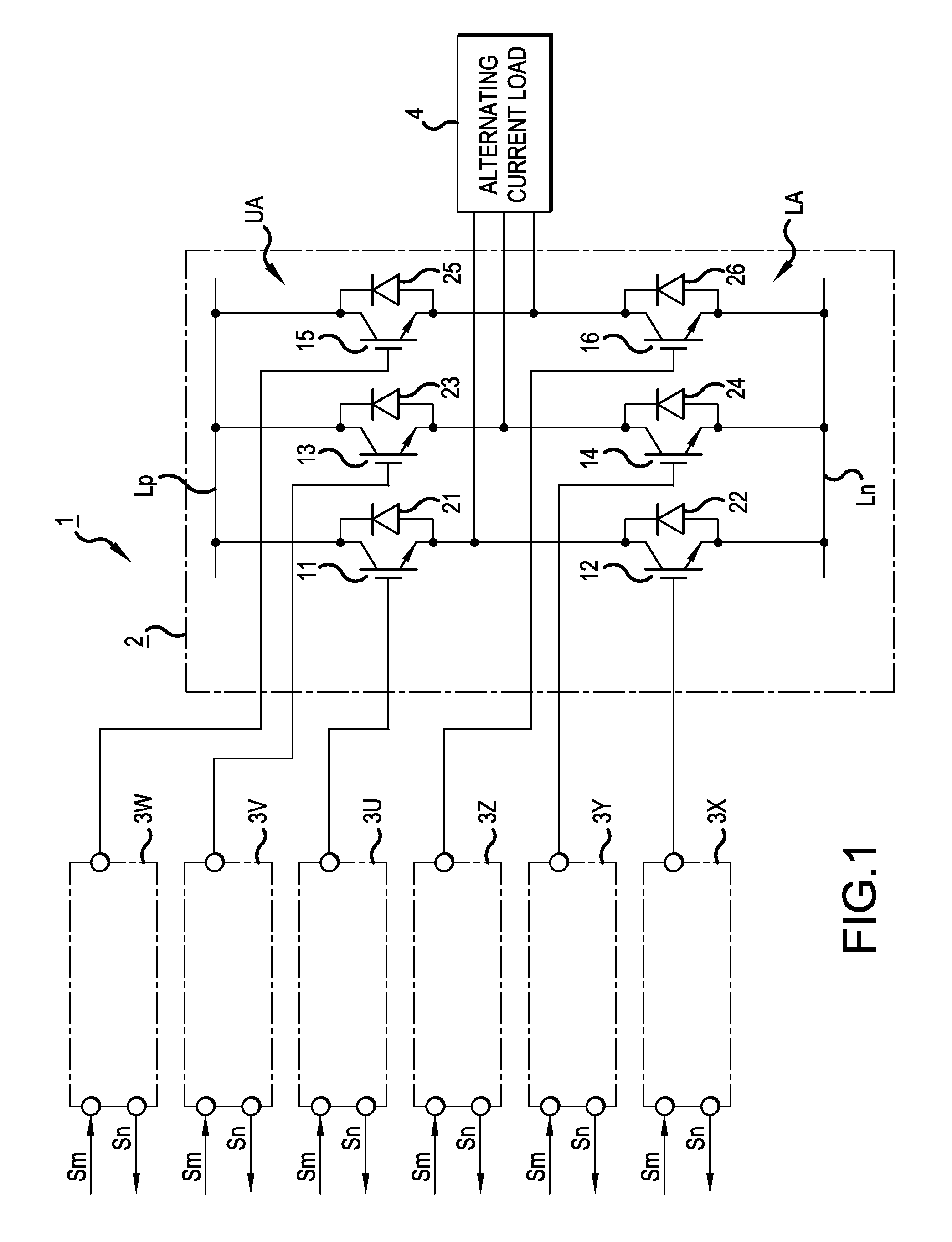
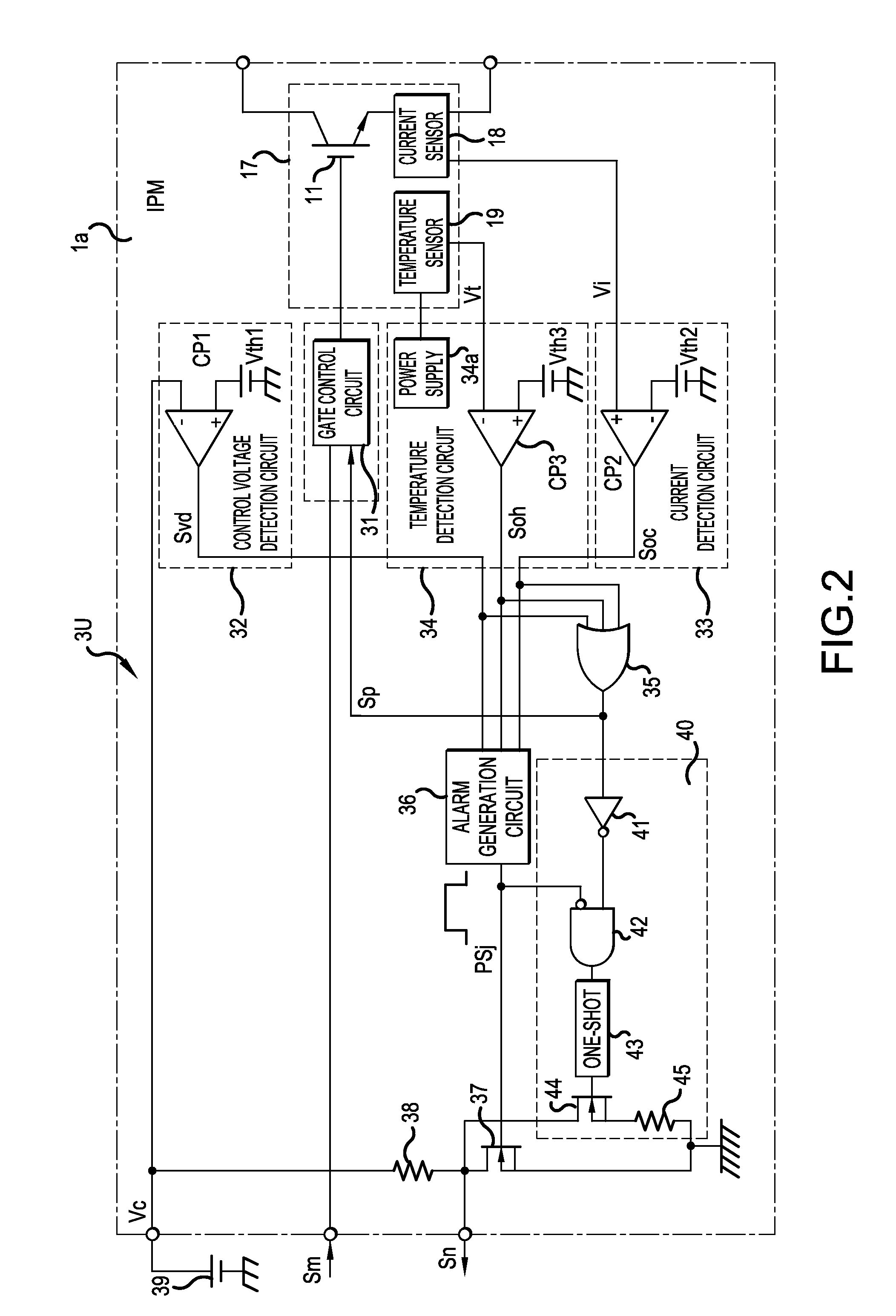
[0023]FIG. 1 is a block diagram showing an overall outline configuration of a power conversion device to which embodiments of the invention may be applied. The power conversion device 1, as well as including an inverter 2 which converts direct current power to alternating current power, includes six drive circuits 3U to 3Z which individually drive a plurality of semiconductor elements, for example, six IGBTs (Insulated Gate Bipolar Transistors) 11 to 16 configuring the inverter 2. Reference numerals 21 to 26 in FIG. 1 show free wheeling diodes respectively connected in reverse parallel between the emitter and collector of the IGBTs 11 to 16.

[0024]The six IGBTs 11 to 16 configuring the inverter 2, by being connected in series by twos, configure three sets of half bridge circuits. The half bridge circuits are interposed between a positive line Lp and negative line Ln of an unshown ...


PUM


Abstract

A semiconductor element drive device includes a drive circuit which drives a semiconductor element configuring a power conversion device; an alarm generation circuit which generates alarm signals with pulse widths corresponding to protection factors in accordance with the outputs of detection circuits which detect information necessary for the operation of protecting the semiconductor element; an output circuit which externally outputs the alarm signals at a predetermined level; a protection cancellation circuit which generates a protection cancellation signal over a fixed period in accordance with the inverting output of a drive stop signal generation circuit, which stops the drive of the semiconductor element by the drive circuit in accordance with the outputs of the detection circuits, and with the output of the alarm generation circuit; and an output control circuit which changes the signal output level of the output circuit in accordance with the protection cancellation signal.

Description

CROSS-REFERENCE TO RELATED APPLICATIONS[0001]This application is a continuation of International Application No. PCT / JP2013 / 079645, filed on Oct. 31, 2013, and is based on and claims priority to Japanese Patent Application No. JP 2012-255949, filed on Nov. 22, 2012. The disclosure of the Japanese priority application and the PCT application in their entirety, including the drawings, claims, and the specification thereof, are incorporated herein by reference.BACKGROUND[0002]1. Field[0003]Embodiments of the present invention relate to a semiconductor element drive device which drives a plurality of semiconductor elements configuring a power conversion device and which includes the function of notifying information necessary for protecting the semiconductor elements.[0004]2. Discussion of the Background[0005]Recently, an intelligent power module (IPM) has attracted attention. The intelligent power module is such that protection circuits for protection against anomalies, such as an over...

Claims


Application Information

Patent Timeline
IPC IPC(8): H02H9/02H02H9/04G08B21/18
CPCH02H9/02H02H9/04G08B21/185H02M1/08H02M1/32H02M7/5387H03K17/0828H03K17/18
Inventor SEKIGAWA, KIYOSHI
Owner FUJI ELECTRIC CO LTD
Why Eureka
Try Eureka