Display device

a display device and panel technology, applied in semiconductor devices, identification means, instruments, etc., can solve the problems of resin not being fully cured, light not reaching the pad region where the fpcb is mounted, and the bonding defect is likely to occur, so as to prevent or reduce the effect of bonding defects

Active Publication Date: 2015-07-02
SAMSUNG DISPLAY CO LTD
View PDF6 Cites 44 Cited by
  • Summary
  • Abstract
  • Description
  • Claims
  • Application Information

AI Technical Summary

Benefits of technology

[0012]Aspects of embodiments of the present invention are directed toward a display device. Further, aspects of embodiments of the present invention are directed toward a display device that can effectively prevent or reduce a bonding defect due to a window by allowing light to be irradiated to an entire region of a resin so as to cure the resin.

Problems solved by technology

However, because light irradiated from the outside of the panel does not readily pass through the black matrix, the resin under the black matrix is not well-cured, and thus, a bonding defect between the panel and the window is likely to occur.
However, even light irradiated from the sides of the window is blocked by a flexible printed circuit board (FPCB), and thus, the light frequently fails to reach a pad region in which the FPCB is mounted.
In this case, the resin may not be fully cured because the light irradiated from the sides is blocked by the FPCB and fails to be incident on the resin.

Method used


Image

  • Display device
  • Display device
  • Display device

Examples


Embodiment Construction

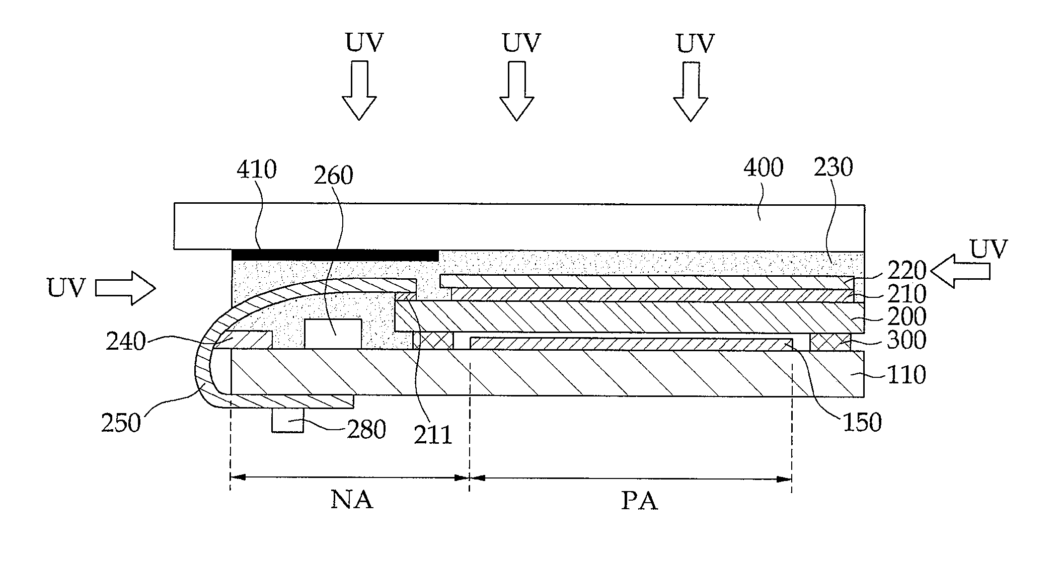
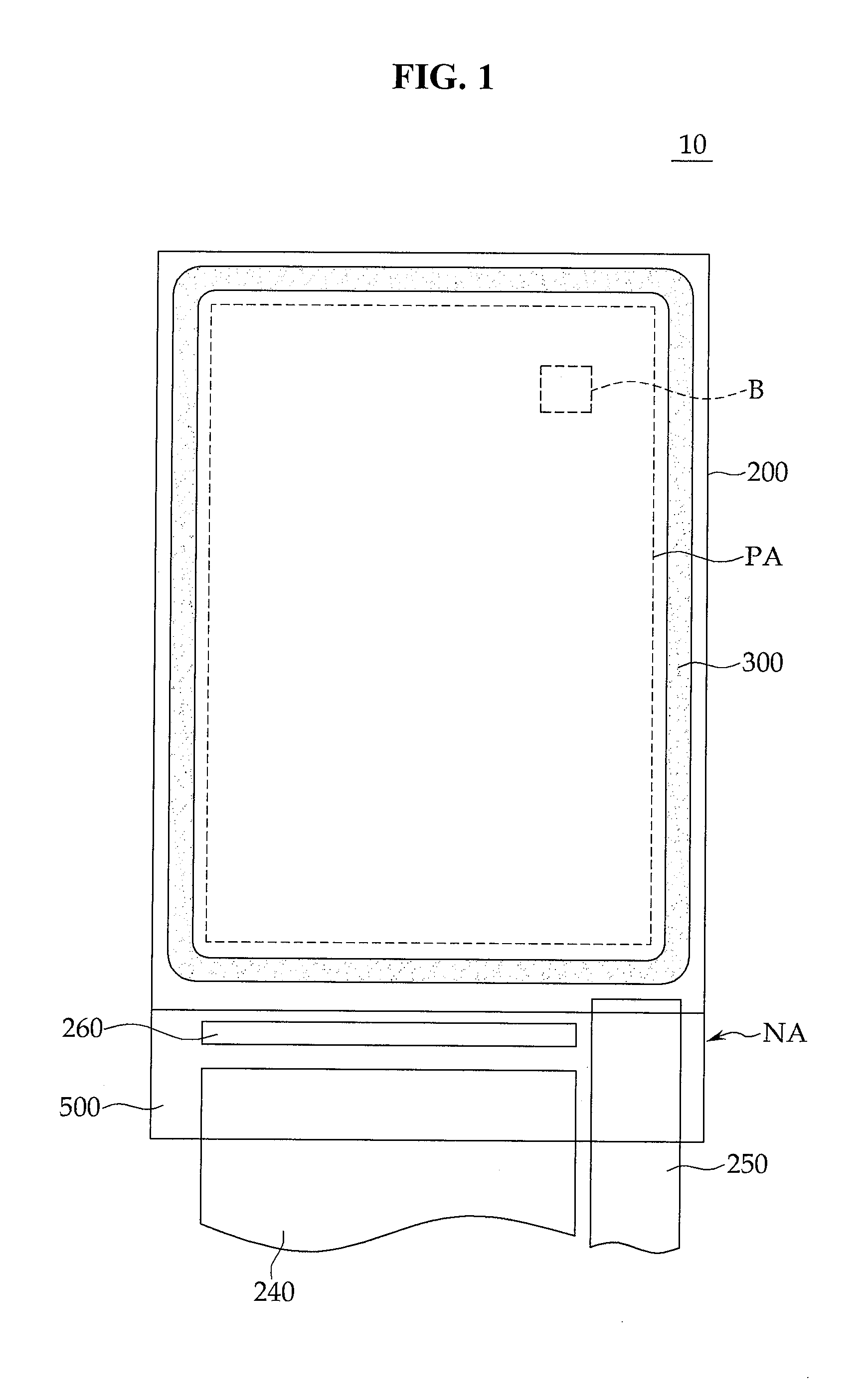
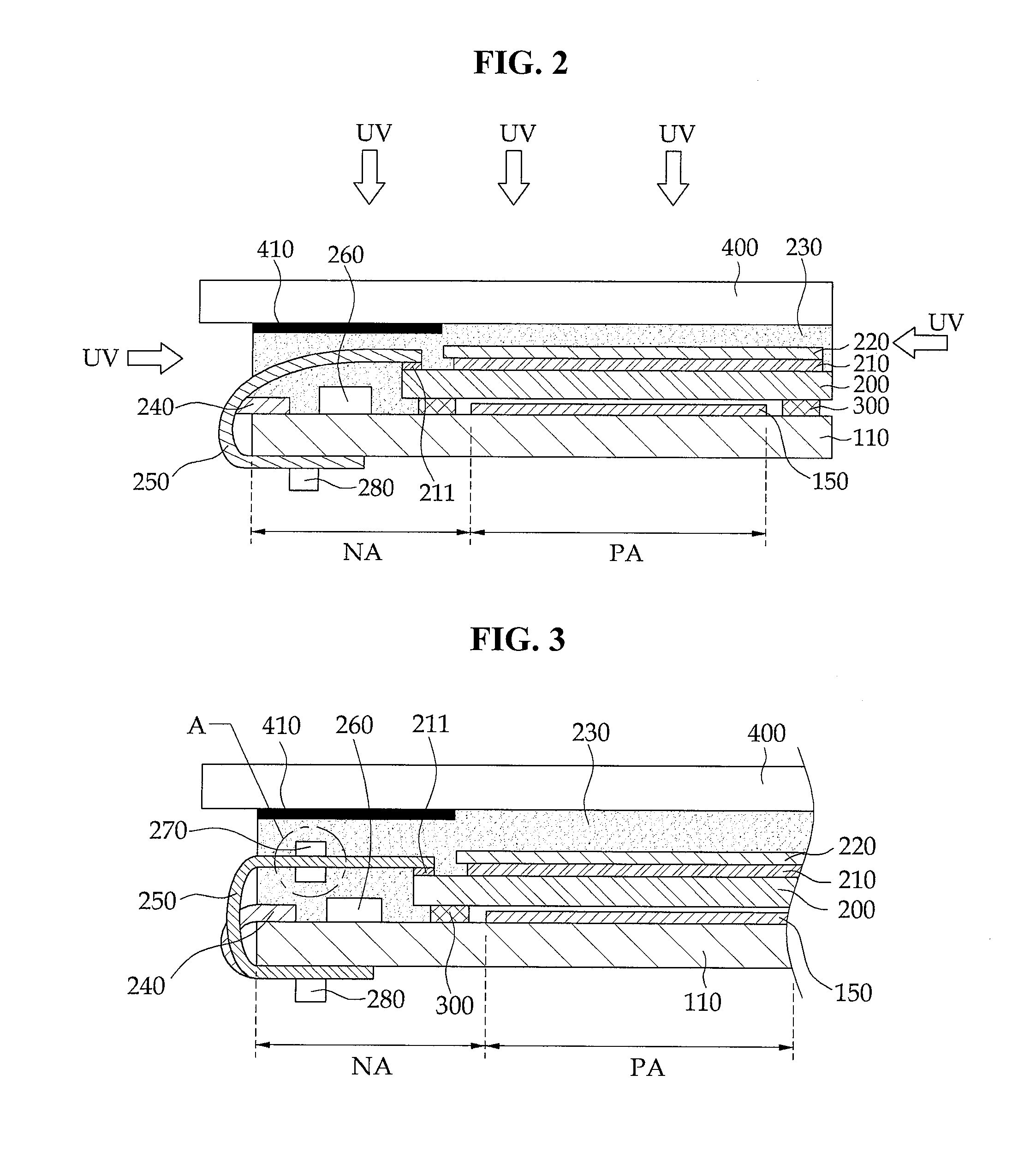
[0044]Characteristics and features of the present invention and methods for achieving them will be made clear from embodiments described below in detail with reference to the accompanying drawings. The present invention may, however, be embodied in many different forms and should not be construed as being limited to the embodiments set forth herein. Rather, these embodiments are provided so that this disclosure will be thorough and complete and will fully convey the scope of the invention to those skilled in the art. However, the present invention should not be limited to the embodiments described herein. Well-known constituent elements, operations, and techniques are not described in detail in the embodiments in order to prevent the present invention from being obscurely interpreted. Like reference numerals refer to like elements throughout the specification.

[0045]The spatially relative terms, such as “below”, “beneath”, “lower”, “above”, “upper”, and the like, may be used herein f...


PUM

PropertyMeasurementUnit
heightaaaaaaaaaa
heightaaaaaaaaaa
total heightaaaaaaaaaa

Abstract

A display device includes: a first substrate including a display area and a pad area; a second substrate facing the first substrate; a touch unit on the second substrate; a window on the touch unit, the window covering the display area and the pad area; an adhesive layer between the window and the touch unit and under the window at the pad area; and a first light source unit under the window at the pad area.

Description

CROSS-REFERENCE TO RELATED APPLICATION[0001]This application claims priority to and the benefit of Korean Patent Application No. 10-2013-0165539, filed on Dec. 27, 2013 in the Korean Intellectual Property Office, the disclosure of which is incorporated herein in its entirety by reference.BACKGROUND[0002]1. Field[0003]Aspects of embodiments of the present invention relate to a display device.[0004]2. Description of the Related Art[0005]In general, flat panel displays, such as liquid crystal displays and organic light emitting diode displays, include a pair of electric field generating electrodes and an electro-optical active layer interposed therebetween. In the liquid crystal display, a liquid crystal layer is included as the electro-optical active layer, and in the organic light emitting diode display, an organic light emitting layer is included as the electro-optical active layer.[0006]One of the pair of electric field generating electrodes is generally coupled to (e.g., connected...

Claims


Application Information

Patent Timeline
Patent Type & Authority Applications(United States)
IPC IPC(8): G02F1/1333H01L27/32G02F1/1335
CPCG02F1/13338G02F1/133305G02F2001/133357H01L27/323G02F1/133512G02F1/133308G02F2201/086G02F2202/023G02F2202/28G02F1/133311G02F1/133331H10K59/40H10K59/126H10K59/131H10K50/841H10K50/8426H10K59/87G09F9/00H10K50/84
Inventor CHANG, SE-IN
Owner SAMSUNG DISPLAY CO LTD
Why Eureka
Try Eureka