Defect inspection device for display panel and method for the same

a display panel and inspection device technology, applied in the field of display panel defects inspection, can solve the problems of reducing the inspection capability of display panels, difficult and impractical to completely avoid display defects, and inability to distinguish and easily be missed, so as to enhance the inspection ability of display panels and improve inspection accuracy

Active Publication Date: 2015-07-02
SHENZHEN CHINA STAR OPTOELECTRONICS TECH CO LTD
View PDF1 Cites 6 Cited by
  • Summary
  • Abstract
  • Description
  • Claims
  • Application Information

AI Technical Summary

Benefits of technology

[0016]The defect inspection method and device of the present invention can easily distinguish some defects of the display panel which are difficult to be inspected (e.g., the protrusion or shell cracking at the terminal side of the display panel) to improve the inspection accuracy in order to enhance the defect inspection ability of the display panel.

Problems solved by technology

However, according to conventional manufacturing techniques of display panel, to completely avoid display defects is very difficult and impractical.
However, due to some kinds of defects (e.g., the protrusion or shell cracking at the terminal side of the display panel) that the grayscale difference of the corresponding greyscale image is small when the light source illuminates the display panel so that it is cannot easily be distinguished and easily to be missed.
Thereby, it reduces the defect inspection capability of the display panel.

Method used


Image

  • Defect inspection device for display panel and method for the same
  • Defect inspection device for display panel and method for the same

Examples


Embodiment Construction

[0019]The following content combines with the drawings and the embodiment for describing the present invention in detail. It is obvious that the following embodiments are only some embodiments of the present invention. For the skilled persons of ordinary skill in the art without creative effort, the other embodiments obtained thereby are still covered by the present invention.

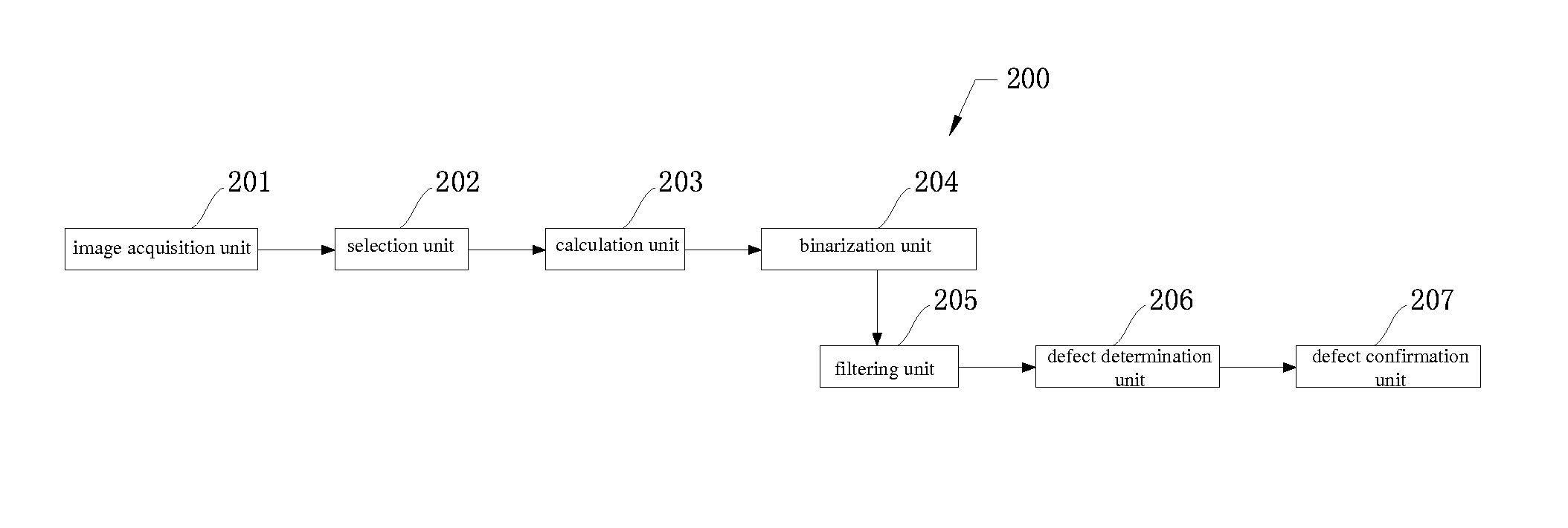
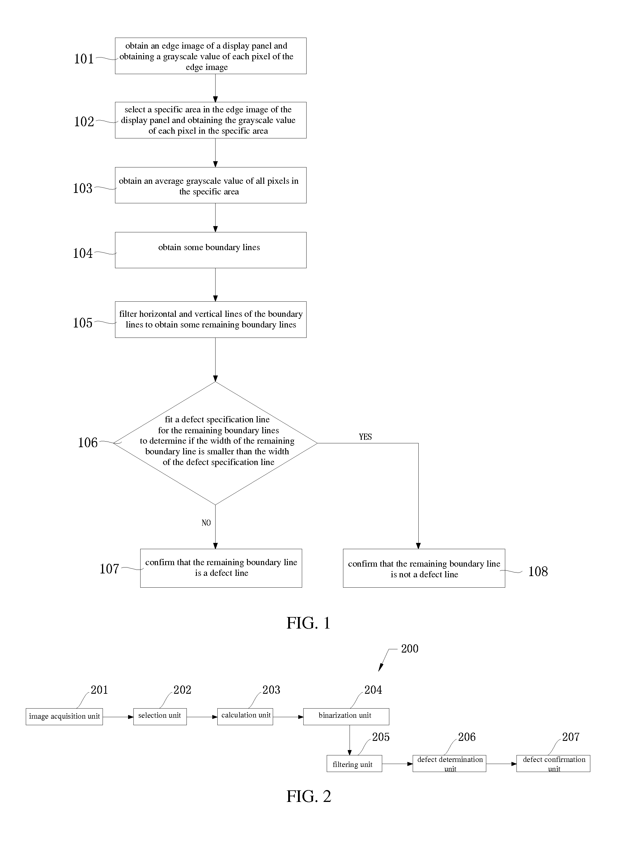
[0020]FIG. 1 is a flowchart of defect inspection method for display panel according to an embodiment of the present invention.

[0021]As shown in FIG. 1, in a step 101, obtaining an edge image of a display panel and obtaining a grayscale value of each pixel of the edge image. For example, utilizing a charge-coupled device (CCD) to scan and capture an image at the edge of the display panel according to the preset parameter to obtain the edge image of the display panel and read the grayscale value of each pixel of the edge image

[0022]In step 102, selecting a specific area in the edge image of the display panel and ...


PUM


Abstract

The present invention provides a defect inspection method and device for a display panel. The defect inspection method comprises: A) obtaining an edge image of the display panel and obtaining a grayscale value of each pixel of the edge image; B) selecting a specific area in the edge image and obtaining a grayscale value of each pixel in the specific area; C) obtaining an average grayscale value of all pixels in the specific area; D) executing binarization for the grayscale value of each pixel in the specific area to obtain some boundary lines based on the average grayscale value, wherein the grayscale values of pixels on the boundary lines are different from grayscale values of the other pixels which are not on the boundary lines; E) filtering horizontal and vertical lines of the boundary lines to obtain some remaining boundary lines; and F) fitting a defect specification line for the remaining boundary lines, wherein, if widths of the remaining boundary lines are not smaller than a width of the defect specification line, confirming that the remaining boundary lines are defect lines.

Description

BACKGROUND OF THE INVENTION[0001]1. Field of the Invention[0002]The present invention relates to the technical field of defect inspection for a display panel; and more particularly to a defect inspection device for a display panel and a method for the same.[0003]2. Description of Related Art[0004]With the rapid development of technology in the display field, the display panel with high-quality image (e.g., LCD panel) has become increasingly popular. However, according to conventional manufacturing techniques of display panel, to completely avoid display defects is very difficult and impractical. Therefore, in the manufacturing process of the display panel, executing a step of display defect inspection for a display panel is necessary.[0005]The prior art, it generally utilize the light source to illuminate the display panel, and obtain a corresponding greyscale image, and then it determines if the display panel exists defect according to if the greyscale image appear the grayscale di...

Claims


Application Information

Patent Timeline
Patent Type & Authority Applications(United States)
IPC IPC(8): G06T7/00
CPCG06T7/0004G06T2207/30121G06T7/0085G06T7/13
Inventor HUANG, HAIBO
Owner SHENZHEN CHINA STAR OPTOELECTRONICS TECH CO LTD
Why Eureka
Try Eureka