Mechanisms for forming finfets with different fin heights

a technology of finfets and fin heights, applied in the direction of semiconductor devices, electrical apparatus, transistors, etc., can solve the problem of more leakage curren

Active Publication Date: 2015-07-02
TAIWAN SEMICON MFG CO LTD
View PDF6 Cites 47 Cited by
  • Summary
  • Abstract
  • Description
  • Claims
  • Application Information

AI Technical Summary

Benefits of technology

[0037]In some embodiments, a semiconductor device is provided. The semiconductor device includes a first fin partially surrounded by a first isolation structure and protruding through a top surface thereof. The semiconductor device also includes a second fin partially surrounded by a second isolation structure and protruding through a top surface thereof. The top surface of the first isolation structure is higher than the top surface of the second isolation structure such that the second fin has a height that is higher than that of the first fin. The second isolation structure has a dopant concentration that is higher than that of the first isolation structure.

Problems solved by technology

However, smaller feature size may lead to more leakage current.

Method used


Image

  • Mechanisms for forming finfets with different fin heights
  • Mechanisms for forming finfets with different fin heights
  • Mechanisms for forming finfets with different fin heights

Examples


Embodiment Construction

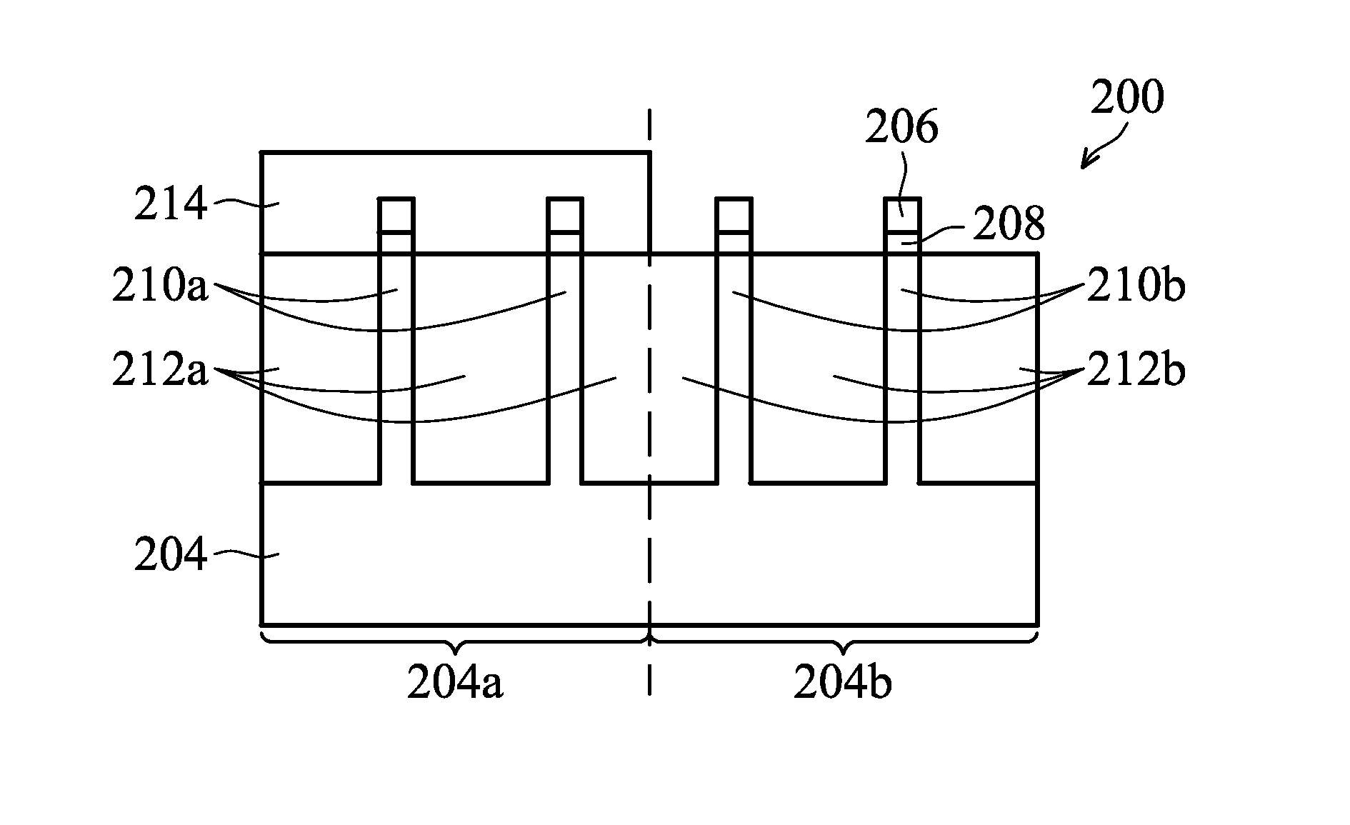
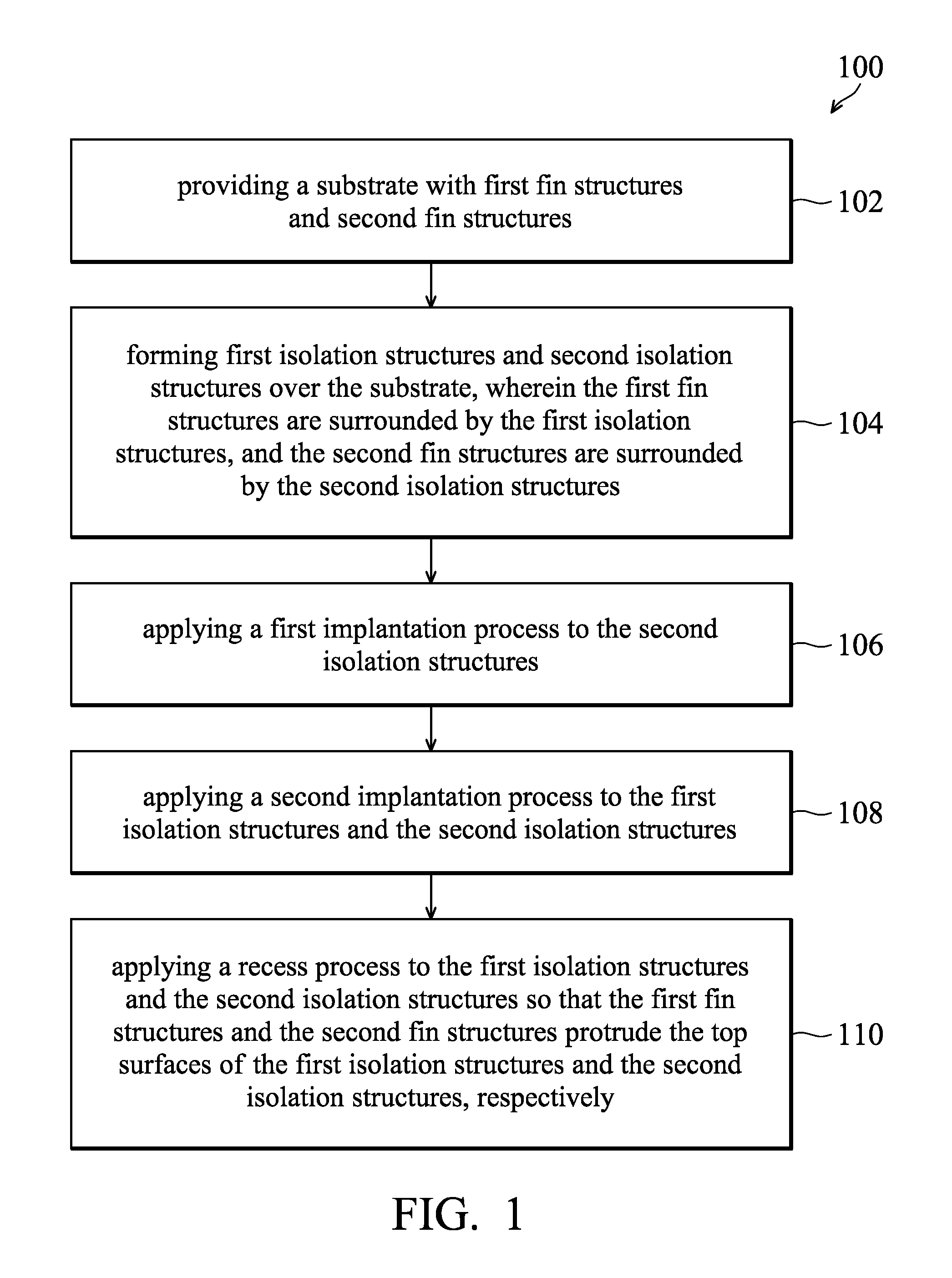
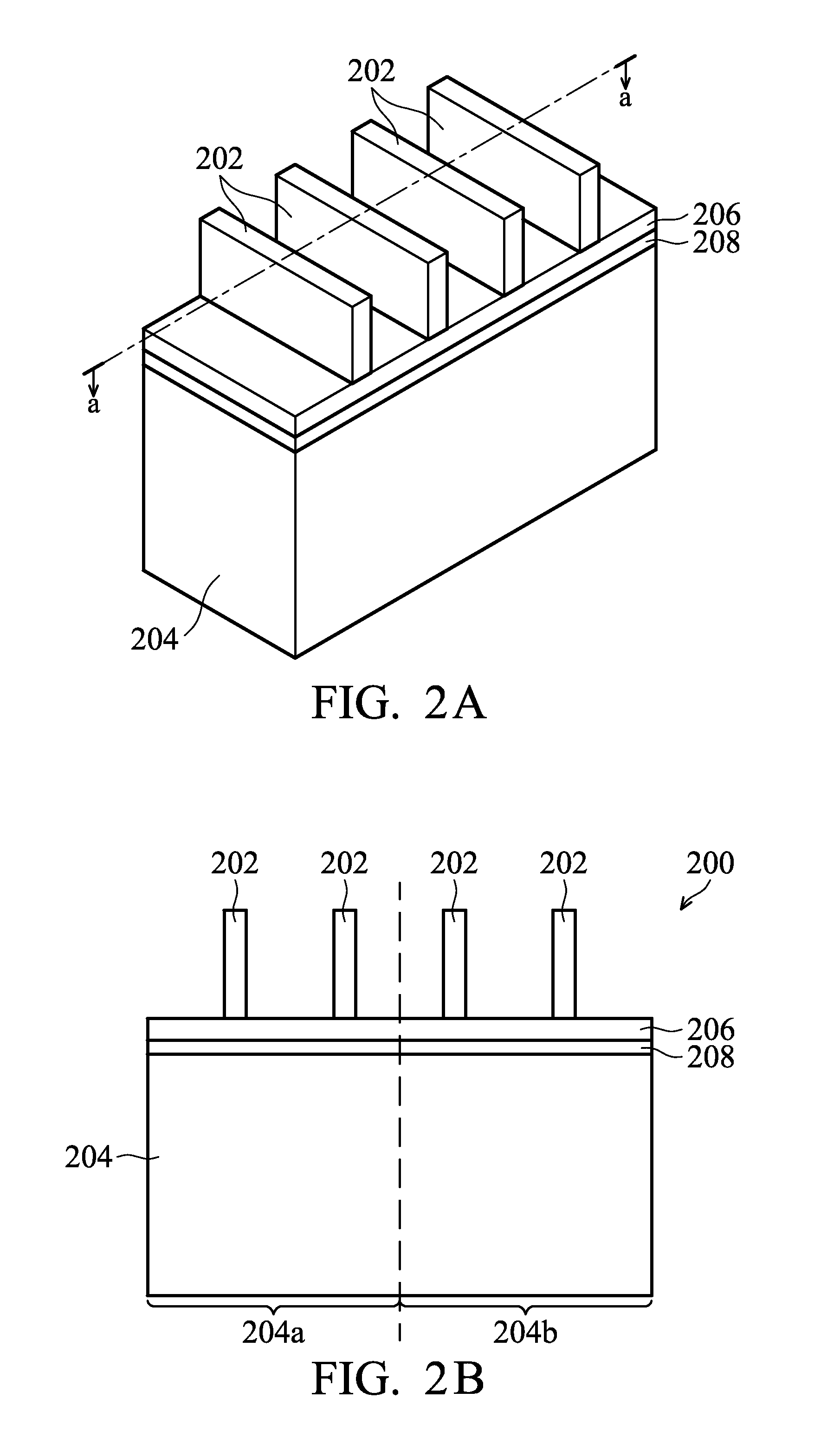
[0007]The making and using of the embodiments of the disclosure are discussed in detail below. It should be appreciated, however, that the embodiments can be embodied in a wide variety of specific contexts. The specific embodiments discussed are merely illustrative, and do not limit the scope of the disclosure.

[0008]It is to be understood that the following disclosure provides many different embodiments, or examples, for implementing different features of the disclosure. Specific examples of components and arrangements are described below to simplify the present disclosure. These are, of course, merely examples and are not intended to be limiting. Moreover, the performance of a first process before a second process in the description that follows may include embodiments in which the second process is performed immediately after the first process, and may also include embodiments in which additional processes may be performed between the first and second processes. Various features m...


PUM


Abstract

Embodiments of mechanisms for forming a semiconductor device are provided. The semiconductor device includes a first fin partially surrounded by a first isolation structure and protruding through a top surface thereof. The semiconductor device also includes a second fin partially surrounded by a second isolation structure and protruding through a top surface thereof. The top surface of the first isolation structure is higher than the top surface of the second isolation structure such that the second fin has a height higher than that of the first fin. The second isolation structure has a dopant concentration higher than that of the first isolation structure.

Description

BACKGROUND[0001]The semiconductor industry has been experiencing rapid growth due to continuous improvements in the integration density of various electronic components (e.g., transistors, diodes, resistors, capacitors, etc.). For the most part, this improvement in integration density has come from repeated reductions in minimum feature sizes, which allows more components to be integrated into a given area. However, smaller feature size may lead to more leakage current. As the demand for even smaller electronic devices has grown recently, there is a need for reducing leakage current in semiconductor devices.[0002]The so called Fin field effect transistor (FinFET) device is becoming increasing popular. The FinFET device is fabricated with a thin fin-like structure called a “fin”, extending from a substrate, and a gate provided over (e.g., wrapping around) the fin. The fin structure is made of semiconductor material, typically silicon, and if used as a transistor, has a current channe...

Claims


Application Information

Patent Timeline
Patent Type & Authority Applications(United States)
IPC IPC(8): H01L21/762H01L21/263H01L21/266H01L27/088H01L29/06
CPCH01L21/76224H01L27/0886H01L21/2636H01L21/76237H01L21/266H01L29/0649H01L21/31111H01L21/31116H01L21/31155H01L21/823431H01L21/823481H01L21/845H01L27/1211H01L29/0653H01L29/66795H01L29/785
Inventor CHIANG, TSUNG-YULIN, CHUNG-WEICHEN, KUANG-HSINTIEN, BOR-ZEN
Owner TAIWAN SEMICON MFG CO LTD
Why Eureka
Try Eureka