Semiconductor device

a technology of semiconductor devices and semiconductors, applied in semiconductor devices, electrical devices, instruments, etc., can solve the problems of large occupation area of inverted staggered transistors, image quality degradation of display devices, etc., and achieve the effects of signal delay, relatively simple manufacturing process, and low manufacturing cos

Active Publication Date: 2015-07-02
SEMICON ENERGY LAB CO LTD
View PDF0 Cites 24 Cited by
  • Summary
  • Abstract
  • Description
  • Claims
  • Application Information

AI Technical Summary

Benefits of technology

[0006]As a transistor including an oxide semiconductor film, an inverted staggered transistor (also referred to as a transistor having a bottom-gate structure), a planar transistor (also referred to as a transistor having a top-gate structure), and the like are given. In the case where a transistor including an oxide semiconductor film is used for a display device, an inverted staggered transistor is used more often than a planar transistor because a manufacturing process thereof is relatively simple and manufacturing cost thereof can be kept low. However, signal delay or the like is increased by parasitic capacitance that exists between a gate electrode and source and drain electrodes of an inverted staggered transistor and accordingly image quality of a display device degrades, which has posed a problem, as an increase in screen size of a display device proceeds, or a display device is provided with a higher resolution image (for example, a high-resolution display device typified by 4k×2k pixels (3840 pixels in the horizontal direction and 2048 pixels in the perpendicular direction) or 8k×4k pixels (7680 pixels in the horizontal direction and 4320 pixels in the perpendicular direction)). Furthermore, as another problem, the occupation area of an inverted staggered transistor is larger than that of a planar transistor. Thus, with regard to a planar transistor including an oxide semiconductor film, development of a transistor which has a structure with stable semiconductor characteristics and high reliability and which is formed by a simple manufacturing process is desired.
[0007]In view of the foregoing problems, one embodiment of the present invention is to provide a novel semiconductor device including an oxide semiconductor, particularly to provide a planar type semiconductor device including an oxide semiconductor. Furthermore, another object is to provide a semiconductor device including an oxide semiconductor in which on-state current is high, provide a semiconductor device including an oxide semiconductor in which off-state current is low, provide a semiconductor device including an oxide semiconductor which occupies a small area, provide a semiconductor device including an oxide semiconductor which has a stable electrical characteristic, provide a semiconductor device including an oxide semiconductor which has high reliability, provide a novel semiconductor device, or provide a novel display device.
[0011]The conductivity of the oxide semiconductor film is increased by containing at least one impurity element. Thus, when a region including the impurity element is provided in a region which does not overlap with the gate electrode, the source electrode, and the drain electrode in the oxide semiconductor film, the parasitic resistance of the transistor can be reduced, and the transistor having high on-state current is obtained.
[0014]One embodiment of the present invention can provide a novel semiconductor device including an oxide semiconductor. In particular, a planar type semiconductor device including an oxide semiconductor can be provided. Alternatively, a semiconductor device including an oxide semiconductor in which on-state current is high can be provided, a semiconductor device including an oxide semiconductor in which off-state current is low can be provided, a semiconductor device including an oxide semiconductor which occupies a small area can be provided, a semiconductor device including an oxide semiconductor which has a stable electrical characteristic can be provided, a semiconductor device including an oxide semiconductor which has high reliability can be provided, a novel semiconductor device can be provided, or a novel display device can be provided.

Problems solved by technology

However, signal delay or the like is increased by parasitic capacitance that exists between a gate electrode and source and drain electrodes of an inverted staggered transistor and accordingly image quality of a display device degrades, which has posed a problem, as an increase in screen size of a display device proceeds, or a display device is provided with a higher resolution image (for example, a high-resolution display device typified by 4k×2k pixels (3840 pixels in the horizontal direction and 2048 pixels in the perpendicular direction) or 8k×4k pixels (7680 pixels in the horizontal direction and 4320 pixels in the perpendicular direction)).
Furthermore, as another problem, the occupation area of an inverted staggered transistor is larger than that of a planar transistor.

Method used


Image

  • Semiconductor device
  • Semiconductor device
  • Semiconductor device

Examples


embodiment 1

[0082]In this embodiment, one embodiment of a semiconductor device and a method for manufacturing the semiconductor device will be described with reference to FIGS. 1A and 1B, FIG. 2, FIGS. 3A to 3C, FIGS. 4A to 4C, FIGS. 5A to 5C, FIGS. 6A and 6B, FIGS. 7A to 7D, FIGS. 8A to 8C, FIGS. 9A to 9C, FIGS. 10A to 10C, and FIGS. 11A and 11B.

[0083]In FIGS. 1A and 1B and FIGS. 6A and 6B, a transistor having a top-gate structure is shown as an example of a transistor included in a semiconductor device. Here, a display device is described as an example of the semiconductor device. Furthermore, structures of transistors provided in a driver circuit and a pixel portion of the display device are described.

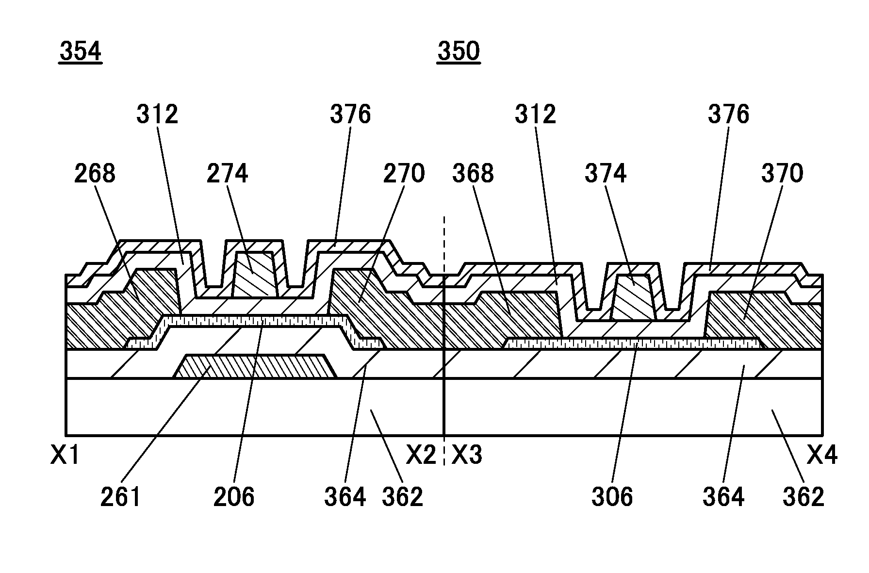
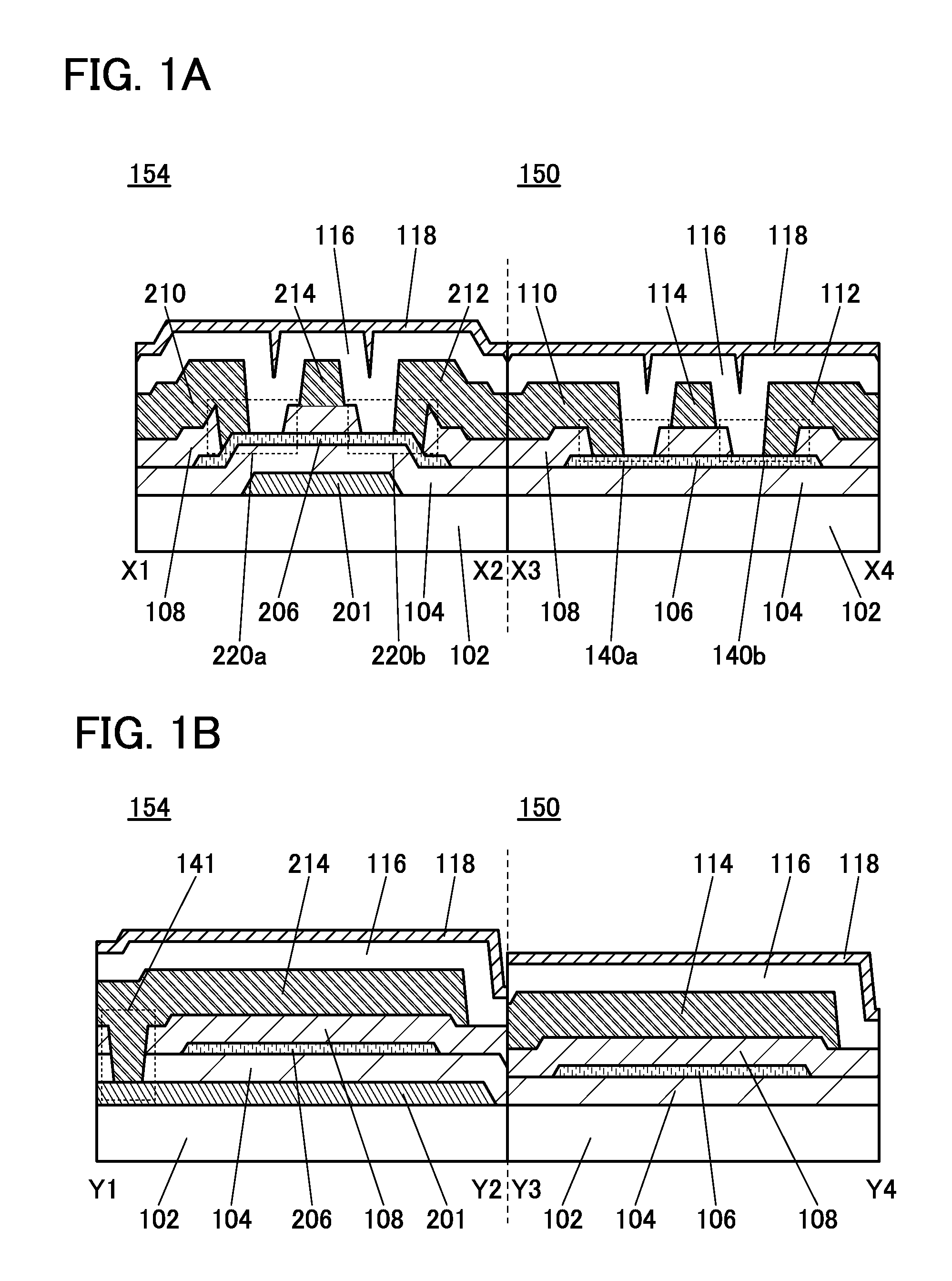
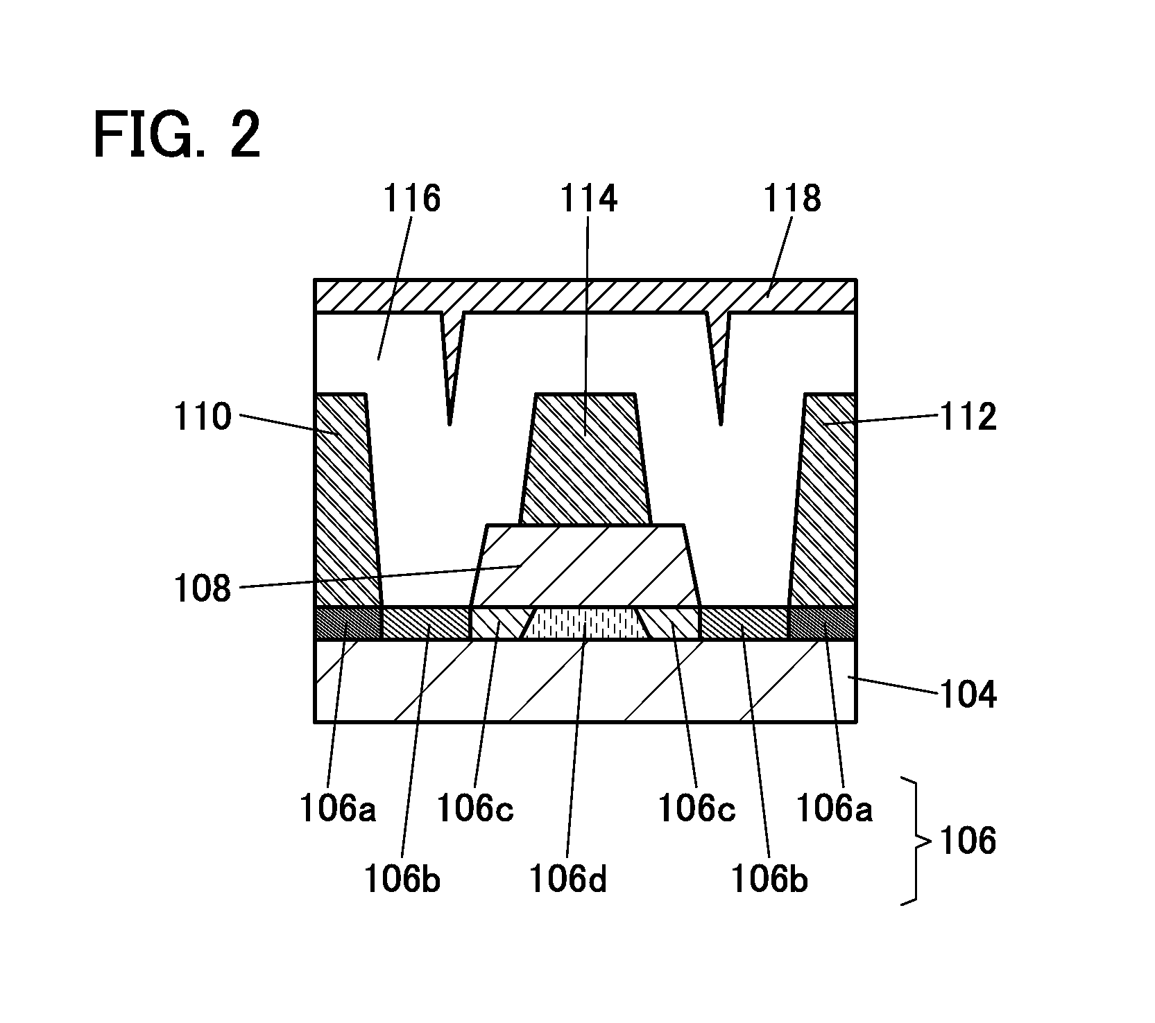
[0084]FIGS. 6A and 6B are top views of a transistor 154 provided in a driver circuit portion and a transistor 150 provided in a pixel portion. FIGS. 1A and 1B are cross-sectional views of the transistor 154 and the transistor 150. FIG. 6A is the top view of the transistor 154, and FIG. 6B is th...

embodiment 2

[0285]In this embodiment, one embodiment of a semiconductor device and a method for manufacturing the semiconductor device will be described with reference to FIGS. 12A and 12B, FIG. 13, FIGS. 14A to 14C, FIGS. 15A to 15C, FIGS. 16A to 16C, FIGS. 17A and 17B, FIGS. 18A and 18B, FIGS. 19A to 19C, FIGS. 20A to 20C, FIGS. 21A to 21C, and FIGS. 22A to 22C. Note that a difference between this embodiment and Embodiment 1 is in a method for forming the low-resistance region.

[0286]In FIGS. 12A and 12B and FIGS. 17A and 17B, a transistor having a top-gate structure is shown as an example of a transistor included in a semiconductor device.

[0287]FIGS. 17A and 17B are top views of a transistor 194 provided in a driver circuit portion and a transistor 190 provided in a pixel portion. FIGS. 12A and 12B are cross-sectional views of the transistor 194 and the transistor 190. FIG. 17A is the top view of the transistor 194, and FIG. 17B is the top view of the transistor 190. FIG. 12A shows cross-sect...

embodiment 3

[0391]In this embodiment, one embodiment of a semiconductor device and a manufacturing method thereof will be described with reference to FIGS. 23A and 23B, FIGS. 24A and 24B, FIGS. 25A to 25C, FIGS. 26A to 26C, FIGS. 27A to 27C, FIGS. 28A and 28B, FIGS. 29A and 29B, FIGS. 30A to 30D, FIGS. 31A to 31C, FIGS. 32A to 32C, FIGS. 33A and 33B, FIGS. 34A to 34D, and FIGS. 35A to 35C. Note that this embodiment differs from Embodiment 1 in that a method for forming a conductive film serving as a gate electrode is different from a method for forming a conductive film serving as a source electrode and a conductive film serving as a drain electrode. Furthermore, as a method for forming a low-resistance region included in a transistor, the method in Embodiment 2 is used.

[0392]In FIGS. 23A and 23B, a transistor having a top-gate structure is shown as an example of a transistor included in a semiconductor device.

[0393]FIGS. 28A and 28B are top views of a transistor 394 provided in a driver circui...


PUM


Abstract

To provide a semiconductor device including a transistor in which an oxide semiconductor is used and on-state current is high. In a semiconductor device including a first transistor provided in a driver circuit portion and a second transistor provided in a pixel portion, the first transistor and the second transistor have different structures. Furthermore, the first transistor and the second transistor are transistors having a top-gate structure in which conductive films serving as a gate electrode, a source electrode, and a drain electrode do not overlap. Furthermore, in an oxide semiconductor film, an impurity element is contained in a region which does not overlap with the gate electrode, the source electrode, and the drain electrode.

Description

TECHNICAL FIELD[0001]One embodiment of the present invention relates to a semiconductor device including an oxide semiconductor and a display device including the semiconductor device.[0002]Note that one embodiment of the present invention is not limited to the above technical field. The technical field of one embodiment of the invention disclosed in this specification and the like relates to an object, a method, or a manufacturing method. In addition, the present invention relates to a process, a machine, manufacture, or a composition of matter. In particular, the present invention relates to a semiconductor device, a display device, a light-emitting device, a power storage device, a storage device, a driving method thereof, or a manufacturing method thereof.[0003]In this specification and the like, a semiconductor device generally means a device that can function by utilizing semiconductor characteristics. A semiconductor element such as a transistor, a semiconductor circuit, an a...

Claims


Application Information

Patent Timeline
Patent Type & Authority Applications(United States)
IPC IPC(8): H01L29/10H01L27/12H01L29/45H01L29/786
CPCH01L29/1033H01L29/7869H01L29/45H01L29/78648H01L29/78696H01L27/1225H01L27/1233H01L27/1251H01L27/1255H10K59/1213H10K59/1216G02F1/133345G02F1/133512G02F1/133514G02F1/13394G02F1/1368H01L27/124H01L29/78606
Inventor YAMAZAKI, SHUNPEIKOEZUKA, JUNICHIJINTYOU, MASAMISHIMA, YUKINORIHAMOCHI, TAKASHINAKAZAWA, YASUTAKA
Owner SEMICON ENERGY LAB CO LTD
Why Eureka
Try Eureka