Matching Process Device, Matching Process Method, and Inspection Device Employing Same

a technology of matching process and inspection device, applied in the field of matching process technology, can solve the problems of large error often caused, and the error of image taken at high magnification ratio by electron microscope, and achieve the effect of accurate matching position

Active Publication Date: 2015-07-16
HITACHI HIGH-TECH CORP
View PDF3 Cites 27 Cited by
  • Summary
  • Abstract
  • Description
  • Claims
  • Application Information

AI Technical Summary

Benefits of technology

[0024]According to the present invention, an accurate matching position can be output in template matching even when there is a large apparent image discrepancy between the template and the searched image.

Problems solved by technology

In the inspection device, while the field of view of the device is moved to a rough position for measuring, a large error is often caused on an image taken at a high magnification ratio by the electron microscope with only the stage positioning accuracy.
Further, the wafer may not be placed on the stage in the same direction every time, and the coordinate system (such as the direction in which wafer chips and the like are arranged) of the wafer placed on the stage may not be completely aligned with the direction in which the stage is driven, creating causes for the error on the image taken at high magnification ratio by the electron microscope.
However, even when the beam shift is performed, an error from the desired observation position may be caused with regard to the irradiation position with only the accuracy of beam deflection control.

Method used


Image

  • Matching Process Device, Matching Process Method, and Inspection Device Employing Same
  • Matching Process Device, Matching Process Method, and Inspection Device Employing Same
  • Matching Process Device, Matching Process Method, and Inspection Device Employing Same

Examples


Embodiment Construction

[0048]In the following, embodiments of the present invention will be described with reference to the drawings. In the drawings, identical reference numerals designate identical members unless otherwise specifically noted.

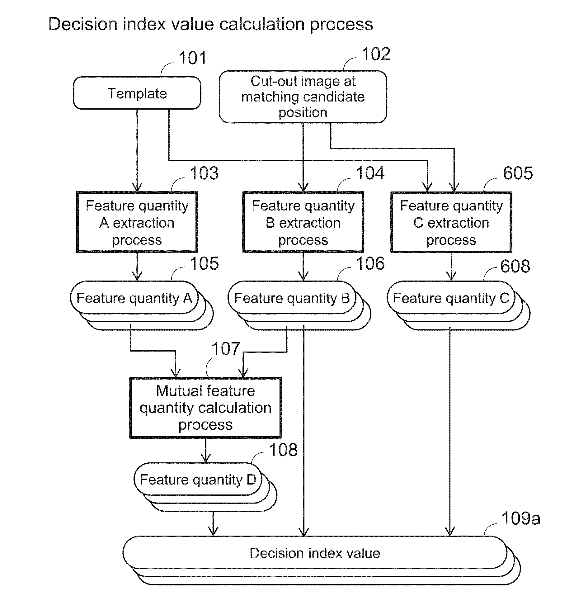
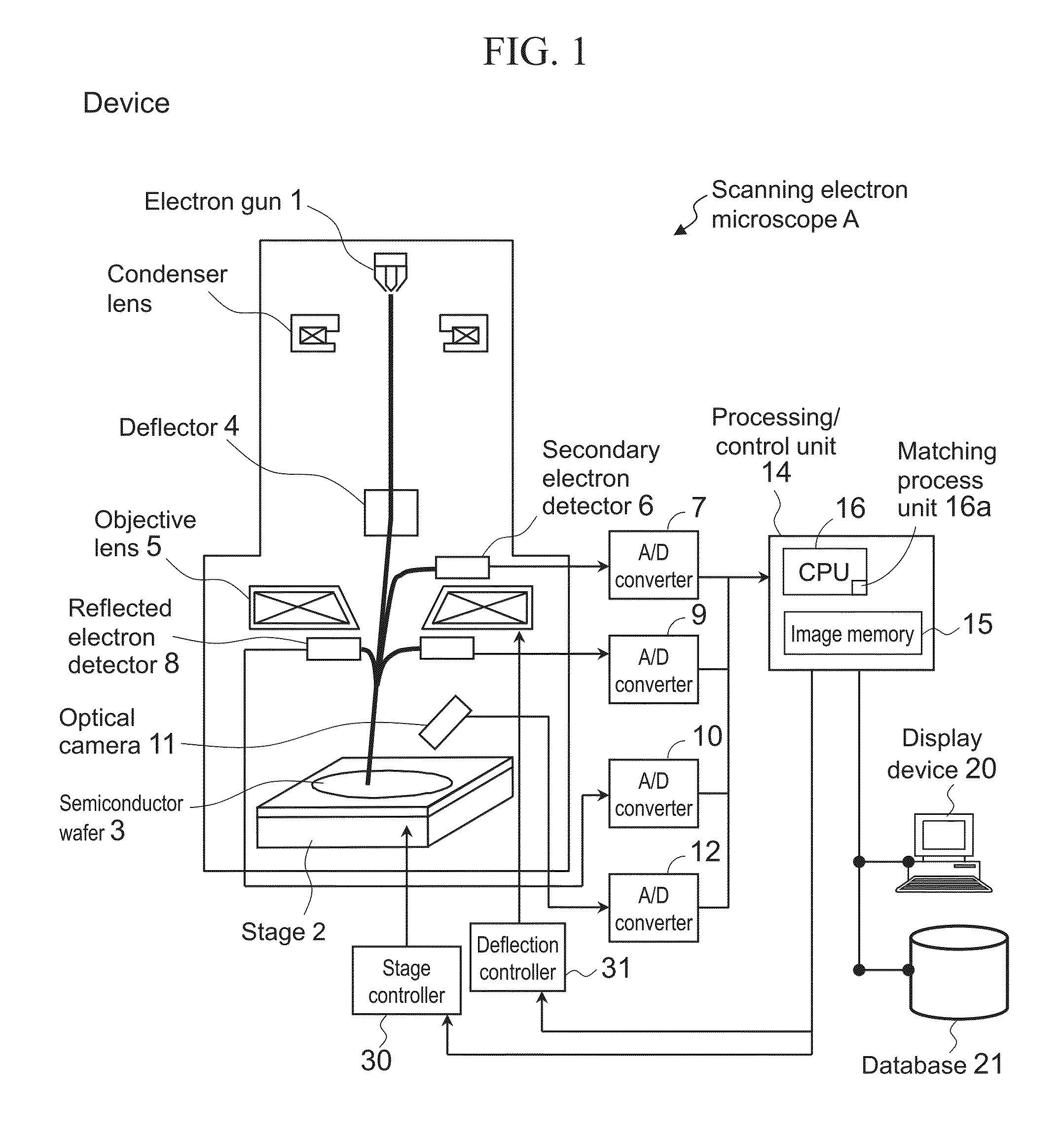
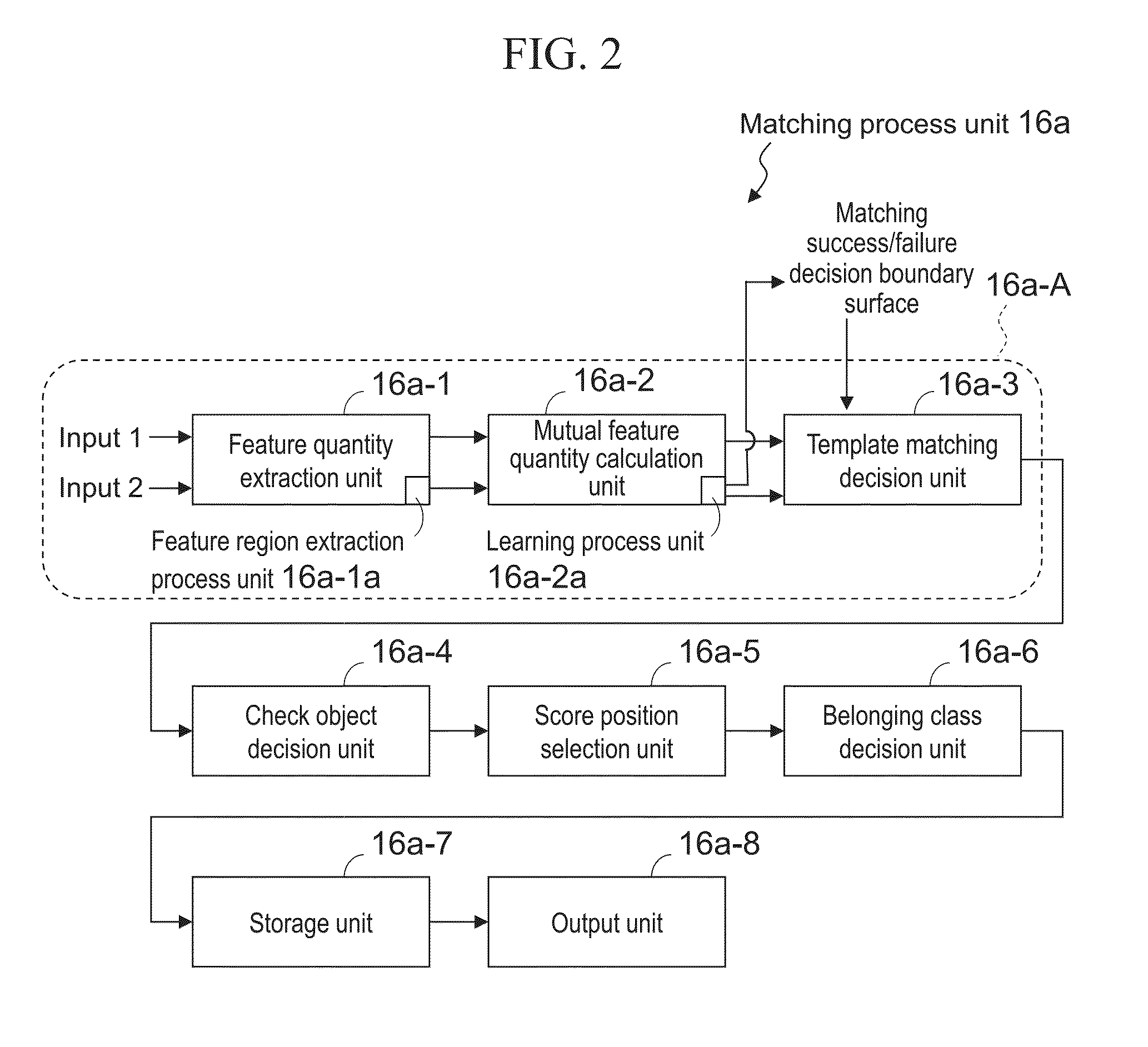
[0049]FIG. 1 illustrates a configuration example of a device for performing template matching using a mask process in a scanning electron microscope (SEM) mainly used for measuring the pattern size of a semiconductor device formed on a semiconductor wafer, as an example of application of an inspection device according to an embodiment of the present invention. In the scanning electron microscope (SEM) A, an electron gun 1 generates an electron beam. The electron beam is focused by controlling a deflector 4 and objective lens 5 so that a sample disposed on a stage 2, such as a semiconductor wafer 3, can be irradiated at a desired position. From the semiconductor wafer 3 irradiated with the electron beam, secondary electrons are emitted, which are detected by a second...


PUM


Abstract

An inspection device that performs pattern matching on a searched image performs matching between a template image of an inspection object and the searched image by using: a feature region extraction process unit that extracts a feature quantity from the template image acquired for learning; a feature quantity extraction process unit that extracts a feature quantity from the searched image acquired for learning; a mutual feature quantity calculation process unit that calculates a mutual feature quantity of the template image and the searched image from the feature quantity extracted from the template image and the feature quantity extracted from the searched image; a learning process unit that calculates, using a plurality of the mutual feature quantities, a discrimination boundary surface that determines matching success or failure; a process unit that calculates a plurality of the mutual feature quantities from an image acquired from the inspection object; and the plurality of mutual feature quantities and the discrimination boundary surface. Thus, an inspection device can be provided that outputs an accurate matching position in template matching even when there is a large apparent image discrepancy between the template and the searched image.

Description

TECHNICAL FIELD[0001]The present invention relates to a matching process technology and more particularly to a pattern matching technology, particularly to a template matching technology in inspection technology for inspection or measurement of a pattern formed on a semiconductor wafer.BACKGROUND ART[0002]In a device for measuring and inspecting a pattern formed on a semiconductor wafer, a process is performed in which the field of view of the inspection device is aligned with a desired measuring position using template matching technology (see Non Patent Literature 1 indicated below) for matching using a template. In Patent Literature 1 indicated below, an example of such template matching method is described. The template matching process refers to a process of finding a region that most closely matches a pre-registered template image from an image as a search object.[0003]In a specific example of the inspection device using template matching, a scanning electron microscope is use...

Claims


Application Information

Patent Timeline
Patent Type & Authority Applications(United States)
IPC IPC(8): G06K9/32G06K9/62G06T7/00G06V10/771
CPCG06K9/3216G06T7/001G06T2207/30148G06T2207/10004G06K9/6215G06T2207/10061G06T2207/20081G01N21/95607G06T7/74G06V20/695G06V10/771G06F18/2113G01N21/956G01N23/225G03F7/70625G06T7/00H01L22/12G06F18/22
Inventor NAGATOMO, WATARUABE, YUICHIUSHIBA, HIROYUKI
Owner HITACHI HIGH-TECH CORP
Why Eureka
Try Eureka