Electronic component

a technology of electronic components and components, applied in the field of electronic components, can solve the problems of difficult to satisfactorily suppress vibration of electronic devices, and achieve the effects of reducing the occurrence of buzzing, and reducing the frequency of buzzing

Active Publication Date: 2015-07-23
TDK CORPARATION
View PDF6 Cites 27 Cited by
  • Summary
  • Abstract
  • Description
  • Claims
  • Application Information

AI Technical Summary

Benefits of technology

[0011]When the electronic component according to the present invention is mounted by soldering on an electronic device, molten solder rises on the third connection electrodes to reach the external electrodes of the multilayer capacitor. Therefore, solder fillets are formed spreading over the electronic device, the interposer, and the multilayer capacitor. At this time, since the first portion is located away from the edge of the first principal surface, the solder rising on the third connection electrode is prevented from spreading across the edge of the first principal surface directly onto the first portion.
[0012]Furthermore, the width in the third direction of each of the second portion and the third connection electrode is smaller than the width in the third direction of the first portion. For this reason, a solder risen region (a region in which the solder has risen) itself is limited to a narrow range, which makes an amount of the solder reaching the multilayer capacitor (external electrodes) smaller. For these reasons, the formed solder fillets become smaller, so as to reduce the vibration propagating through the solder fillets from the multilayer capacitor to the electronic device. As a result, the occurrence of buzzing is satisfactorily suppressed.
[0013]An area of each second connection electrode may be smaller than an area of each first connection electrode. In this case, the connection area between the interposer and the electronic device becomes smaller, so as to reduce the vibration propagating from the interposer to the electronic device. As a result, the occurrence of buzzing is more satisfactorily suppressed.
[0014]Each third connection electrode may include a region with a narrower width in the third direction, midway in the first direction. In this case, the amount of the solder rising on the third connection electrode becomes much smaller, so as to make the solder fillets much smaller. As a result, the occurrence of buzzing is more satisfactorily suppressed.
[0015]The electronic component may further comprise a resin arranged between the multilayer capacitor and the interposer and connecting the multilayer body and the substrate. In this case, connection strength between the multilayer capacitor and the interposer is enhanced.

Problems solved by technology

For this reason, the electrostrictive vibration occurring in the multilayer capacitor propagates through the solder in the recesses to the electronic device and can cause vibration of the electronic device.
Namely, it is difficult to satisfactorily suppress the occurrence of buzzing, in the case of the electronic component described in Patent Literature 1.

Method used


Image

  • Electronic component
  • Electronic component
  • Electronic component

Examples


Embodiment Construction

[0034]The embodiment of the present invention will be described below in detail with reference to the accompanying drawings. In the description, identical elements or elements with identical functionality will be denoted by the same reference signs, without redundant description.

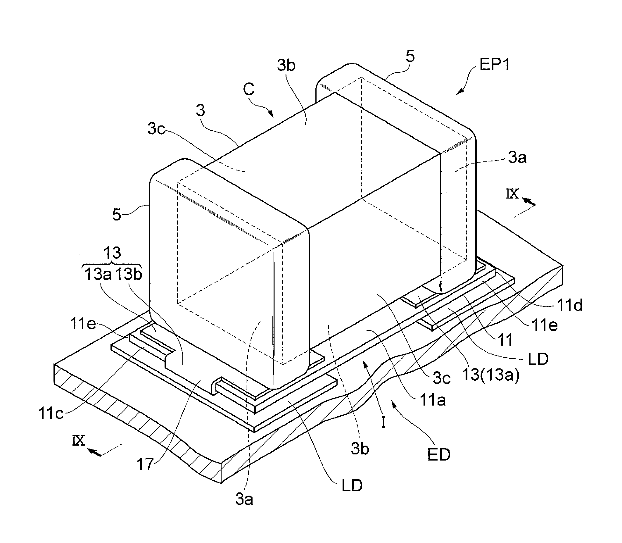
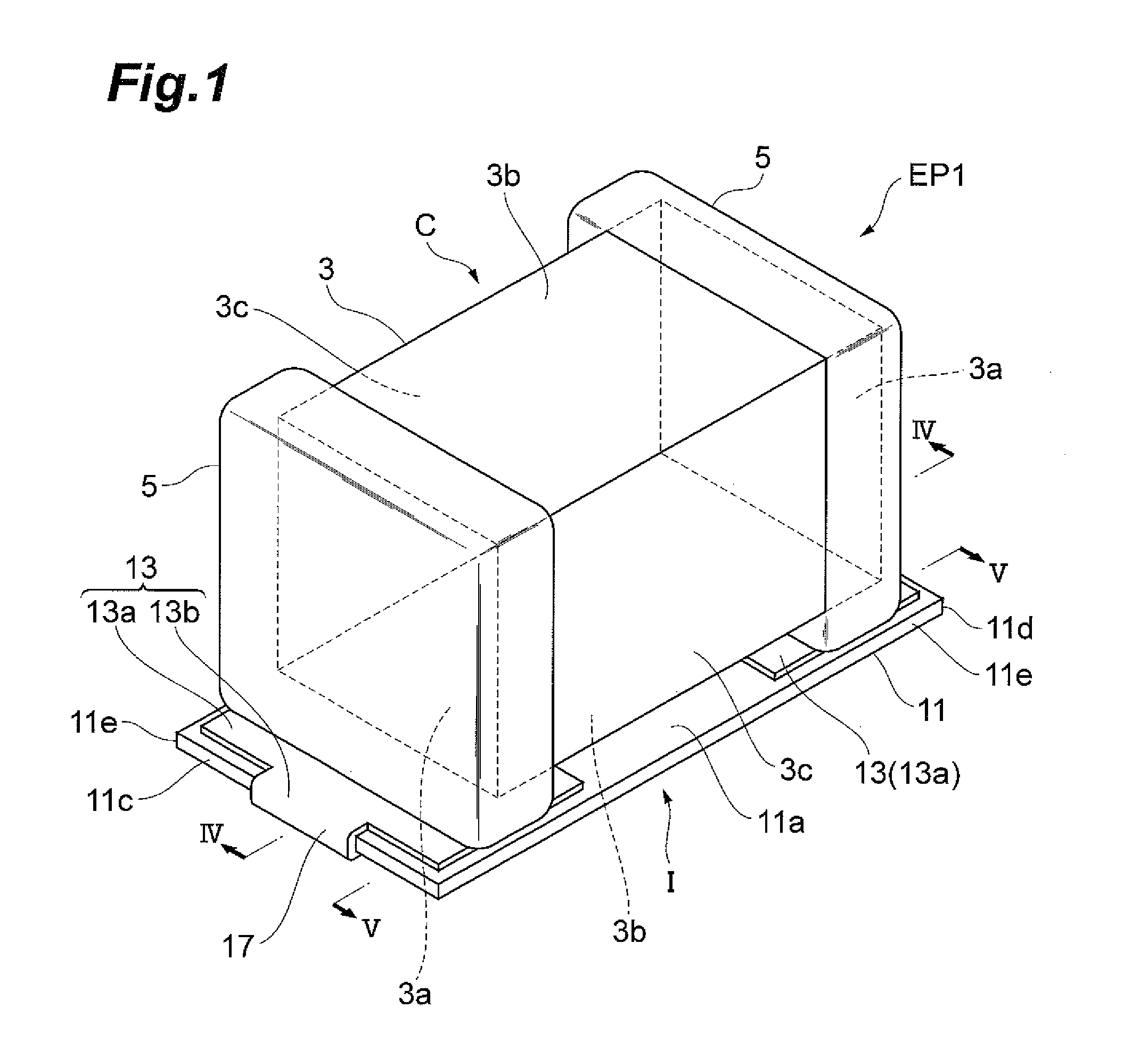
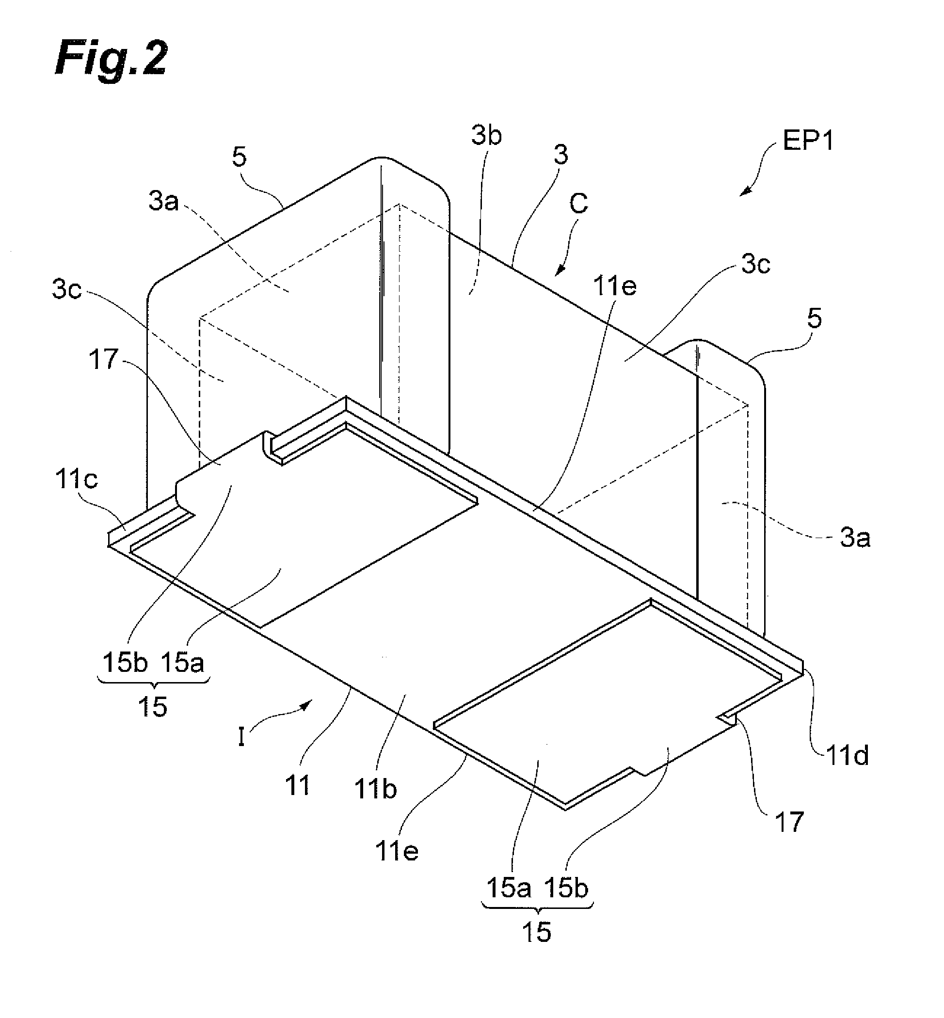
[0035]A configuration of an electronic component EP1 according to the present embodiment will be described with reference to FIGS. 1 to 5. FIGS. 1 to 3 are perspective views showing the electronic component according to the present embodiment. FIG. 4 is a drawing for explaining a cross-sectional configuration along the line IV-IV in FIG. 1. FIG. 5 is a drawing for explaining a cross-sectional configuration along the line V-V in FIG. 1.

[0036]The electronic component EP1, as shown in FIGS. 1 to 5, has a multilayer capacitor C and an interposer I. In the present embodiment, the multilayer capacitor C and the interposer I are connected by solder S. Namely, the multilayer capacitor C is mounted by soldering on th...


PUM

PropertyMeasurementUnit
thicknessaaaaaaaaaa
shapeaaaaaaaaaa
widthaaaaaaaaaa

Abstract

An interposer includes a plurality of first connection electrodes each of which is arranged on either of first- and second-side-surface sides of a first principal surface of a substrate; a plurality of second connection electrodes each of which is arranged on either of first- and second-side-surface sides of a second principal surface of the substrate; and a plurality of third connection electrodes each of which is arranged on either of first and second side surfaces. Each of the first connection electrodes has a first portion located away from an edge of the first principal surface, and a second portion extending from the first portion to the edge and connected to the third connection electrode. Each of the second portion of each first connection electrode and the plurality of third connection electrodes has a width smaller than a width of the first portion of each first connection electrode.

Description

BACKGROUND OF THE INVENTION[0001]1. Field of the Invention[0002]The present invention relates to an electronic component having a multilayer capacitor and an interposer on which the multilayer capacitor is mounted.[0003]2. Related Background Art[0004]There are known electronic components having a multilayer capacitor and an interposer on which the multilayer capacitor is mounted (e.g., cf. Japanese Patent Application Laid-open Publication No. 2012-204572 (which will be referred to hereinafter as Patent Literature 1)).[0005]When a voltage is applied to a multilayer capacitor, mechanical strain arises in magnitude depending upon the applied voltage in an element body due to an electrostrictive effect. This mechanical strain causes vibration of the multilayer capacitor (which will be referred to hereinafter as electrostrictive vibration). When the multilayer capacitor is mounted on an electronic device (e.g., a circuit board, another electronic component, or the like) and when the volt...

Claims


Application Information

Patent Timeline
Patent Type & Authority Applications(United States)
IPC IPC(8): H01G4/30H01G4/06H01G4/248H01G2/06H01G4/005
CPCH01G4/30H01G2/06H01G4/06H01G4/248H01G4/005H01G4/012H01G4/12H01G4/228H01G4/232H01G4/35
Inventor FUJIMURA, TOMOYOSHISATO, ATSUSHI
Owner TDK CORPARATION
Why Eureka
Try Eureka