
Touch panel and method for manufacturing the same

a technology of touch panel and manufacturing method, which is applied in the field of touch panel, to achieve the effect of improving the overall visibility of the connection electrode and reducing the reflectance of the incident ligh

Active Publication Date: 2015-07-30
LG INNOTEK CO LTD
View PDF3 Cites 12 Cited by
  • Summary
  • Abstract
  • Description
  • Claims
  • Application Information

AI Technical Summary

Benefits of technology

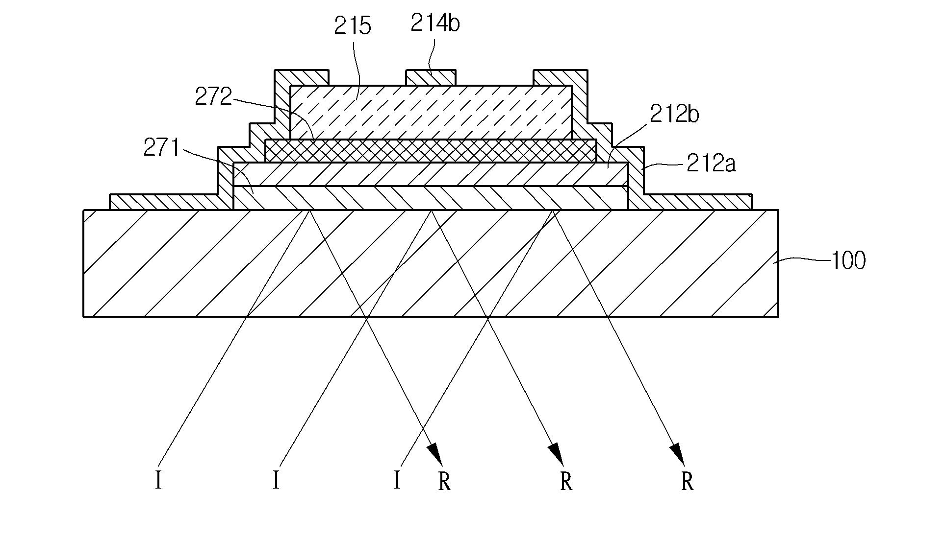
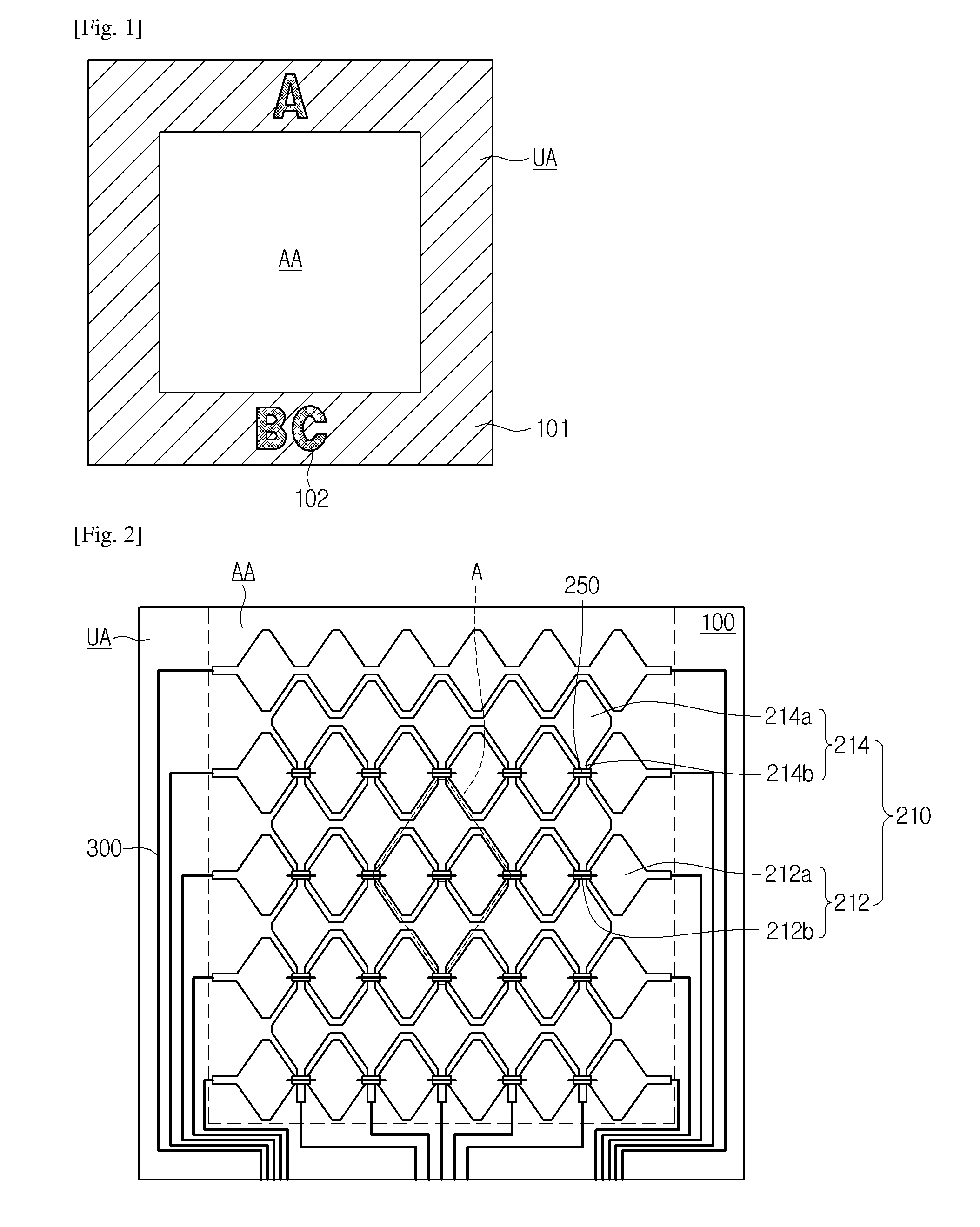
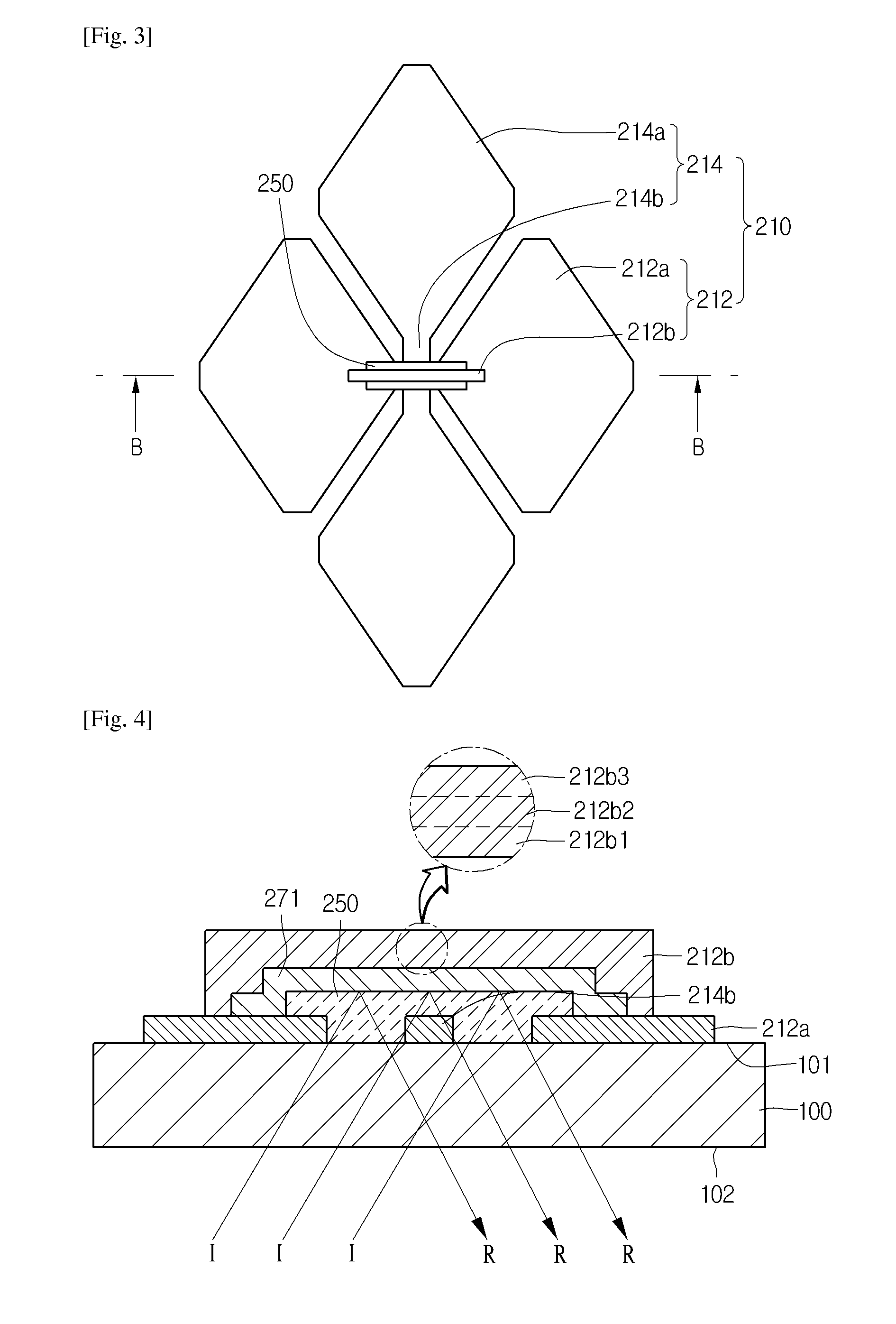
The invention is about improving the visibility of the connection electrode of a touch panel by adding a layer that absorbs light. This prevents the connection electrode from being seen by light that is incident through the substrate. This results in a more visually appealing touch panel.

Problems solved by technology

The touch panel has a problem in that the pattern of a connection electrode may be seen by external incident light or light incident into an LCD provided on the touch panel.

Method used


Image

  • Touch panel and method for manufacturing the same
  • Touch panel and method for manufacturing the same
  • Touch panel and method for manufacturing the same

Examples


embodiment 1

[0054]A sensor part was formed on a glass substrate by depositing indium tin oxide (ITO).

[0055]An insulating layer was formed on the sensor part. A first light absorbing layer was formed on the insulating layer by depositing Mo, Ar, N2 and CO2 through a reactive sputtering process. Accordingly, the first light absorbing layer includes nitride and oxide. A connection electrode including a first buffer layer, a conductive layer, and a second buffer layer was formed by forming the first buffer layer including molybdenum (Mo), the conductive layer including silver (Ag), and the second buffer layer including Mo on the first light absorbing layer.

embodiment 2

[0056]A touch panel according to the second embodiment was manufactured in the same scheme as that of the first embodiment except that a second light absorbing layer was additionally formed in the same scheme as the scheme of forming the first light absorbing layer on the connection electrode.


PUM


Abstract

Disclosed are a touch panel and a method for manufacturing the same. The touch panel includes a touch panel including a substrate, a sensor part on the substrate and a connection electrode connecting the sensor part, and a light absorbing layer on the substrate. The light absorbing layer is closer to the substrate rather than the connection electrode. The method includes preparing a substrate, forming a sensor part and a connection electrode on the substrate, and forming a light absorbing layer on the substrate. The light absorbing layer is closer to the substrate rather than the connection electrode.

Description

TECHNICAL FIELD[0001]The disclosure relates to a touch panel and a method for manufacturing the same.BACKGROUND ART[0002]Recently, a touch panel, which performs an input function through the touch of an image displayed on a display device by an input device such as a stylus pen or a hand, has been applied to various electronic appliances.[0003]The touch panel may be representatively classified into a resistive touch panel and a capacitive touch panel. In the resistive touch panel, the position of the touch point is detected by detecting the variation of resistance according to the connection between electrodes when pressure is applied to an input device. In the capacitive touch panel, the position of the touch point is detected by detecting the variation in capacitance when a finger of the user is touched on the capacitive touch panel between electrodes. When taking of the convenience of a fabrication scheme and a sensing power, recently, the capacitive touch panel has been spotligh...

Claims


Application Information

Patent Timeline
Patent Type & Authority Applications(United States)
IPC IPC(8): G06F1/16G06F3/044
CPCG06F3/044G06F1/16G06F3/0416G06F3/045G06F2203/04103G06F3/0412G06F3/0445G06F2203/04111G06F3/041
Inventor HONG, BEOM SUNKIM, JA RAMLEE, DONG KEONLEE, JAE HONG
Owner LG INNOTEK CO LTD
Learn More