Manufacture of semiconductor device

a manufacturing method and semiconductor technology, applied in the direction of semiconductor devices, basic electric elements, electrical appliances, etc., can solve the problems of deterioration of the performance the high integration of the semiconductor device (semiconductor integrated circuit device), and the downsizing of the semiconductor device, so as to achieve the effect of activation

Inactive Publication Date: 2010-11-16
RENESAS ELECTRONICS CORP
View PDF16 Cites 1 Cited by
  • Summary
  • Abstract
  • Description
  • Claims
  • Application Information

AI Technical Summary

Benefits of technology

[0027]Another object of the present invention is to provide a technology capable of effectively performing the impurity activation by using laser annealing to an SiC substrate.
[0030]In the method of manufacturing a semiconductor device according to the present invention, first, low-concentration semiconductor regions (extension of source and drain) each having a part located below a gate electrode are formed by performing ion-implantation to a semiconductor substrate. Then, after sidewall insulators are formed on the sidewalls of the gate electrode, high-concentration semiconductor regions (source and drain) are formed by performing ion-implantation. Subsequently, a reflectance-controlling layer having a thickness controlled so as to minimize the reflectance of annealing light on a first region and maximize the reflectance of annealing light on a second region is formed on the entire surface of the substrate. Then, a long-wavelength laser annealing treatment with a wavelength of 3 μm or more is performed in order to activate the implanted impurities. In this case, a layer having a complex component k of 1 or more in a complex refractive index n+ik in a wavelength of the light to be used is used as the reflectance-controlling layer.
[0033]Further, in the manufacturing technology of a semiconductor device according to the present invention, impurities can be effectively activated by using laser annealing to an SiC substrate.

Problems solved by technology

This is a disadvantage for the downsizing and the high integration of a semiconductor device (semiconductor integrated circuit device).
However, the reduction of dose amount increases the resistance of a formed impurity diffusion layer, and there is a possibility that performance of a semiconductor device is deteriorated.

Method used


Image

  • Manufacture of semiconductor device
  • Manufacture of semiconductor device
  • Manufacture of semiconductor device

Examples


first embodiment

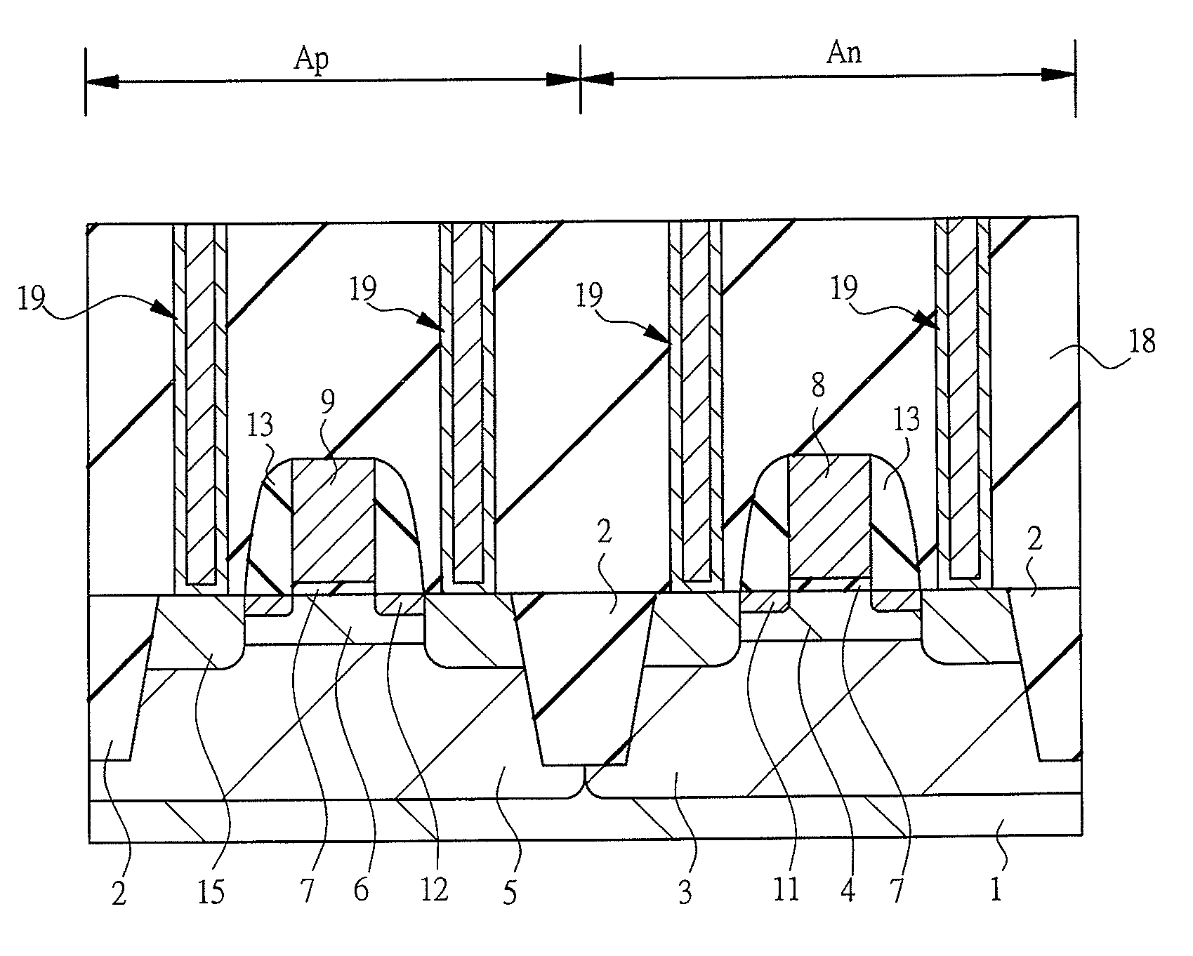
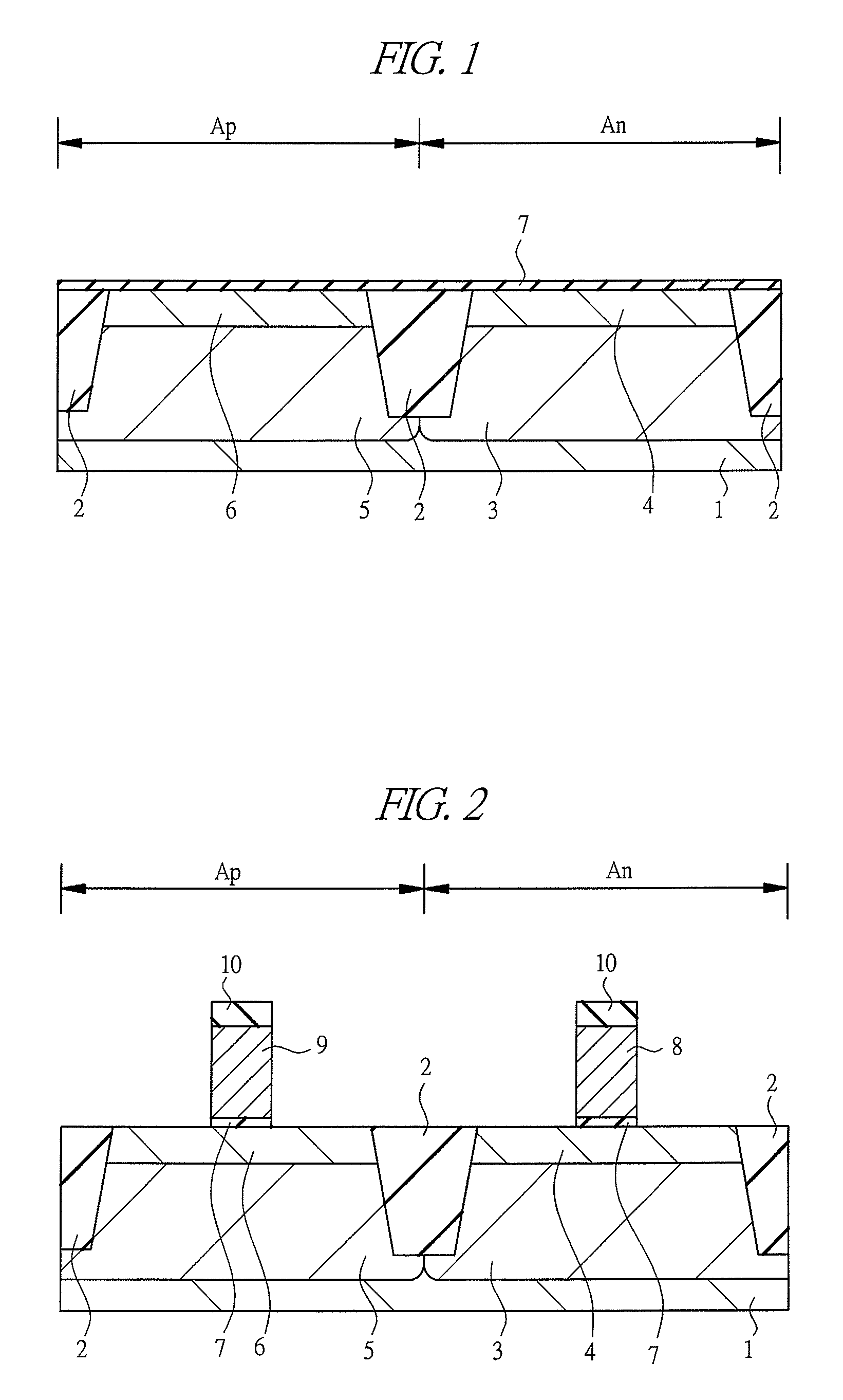
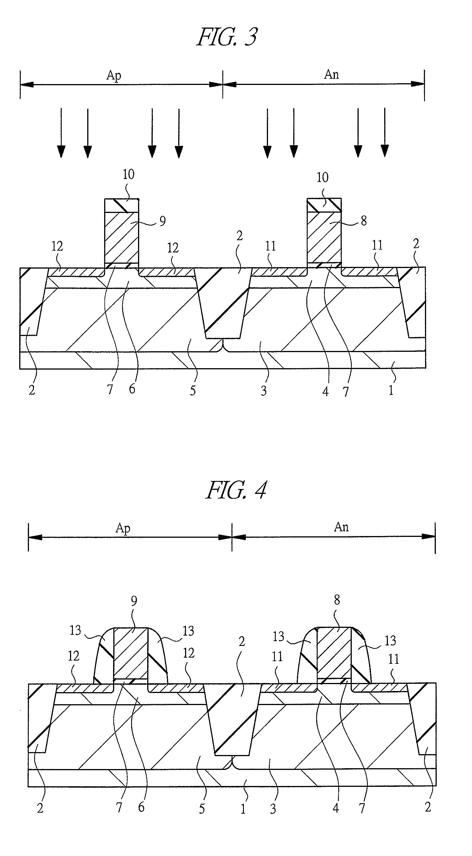
[0056]Manufacturing process of a semiconductor device according to the first embodiment will be described with reference to the drawings. FIG. 1 to FIG. 8 are cross-sectional views showing a principal part of a semiconductor device according to an embodiment of the present invention, for example, the manufacturing process of CMIS.

[0057]First, as shown in FIG. 1, for instance, a semiconductor substrate 1 made of p-type single-crystal silicon and having a resistivity in a range from about 1 to 10 Ωcm is prepared. This semiconductor substrate 1 has a region Ap on which a p-channel MISFET (hereinafter, referred to as pMIS) is formed and a region An on which an n-channel MISFET (hereinafter, referred to as nMIS) is formed. In other words, a pMIS and an nMIS which constitute a CMIS are formed on the main surface of this semiconductor substrate 1.

[0058]Then, an element isolation region 2 is formed in the main surface of the semiconductor substrate 1. The element isolation region 2 is made ...

second embodiment

[0106]In the first embodiment, the case where a silicon dioxide layer is applied to the gate insulator 7 has been described. However, in the second embodiment, the case where a high-k layer is applied to the gate insulator 7 will be described. Since the manufacturing process up to the step of forming the gate insulator 7 is the same as that of the first embodiment, the description thereof will be omitted and the manufacturing process thereafter will be described.

[0107]As shown in FIG. 1, a stacked gate insulator HfSiO2 / HfO2 (high-k layer) with the thickness of about 0.5 nm / 3 nm is formed as the gate insulator 7 on the surface of the p-type well 3 and the n-type well 5 by a sputtering method or a CVD method. A composition ratio of HfSiO2 layer is, for example, Si / (Si+Hf)=10 to 50 atom %.

[0108]Next, as shown in FIG. 2, a metal layer made of Al, W, Ti or nitrides of these metals to be the gate electrodes 8 and 9 is formed by a sputtering method or a CVD method. For example, its thickne...

third embodiment

[0117]In the first embodiment, the case where the annealing treatment according to the present invention is applied to the process of activating impurities has been described. However, in the third embodiment, the case where it is applied to the siliciding step will be described.

[0118]FIG. 17 and FIG. 18 are sectional views showing the principal part in the manufacturing process of a semiconductor device according to the third embodiment. Since the manufacturing process up to the step shown in FIG. 7 is the same as that of the first embodiment, the description thereof will be omitted and the manufacturing process thereafter will be described.

[0119]As shown in FIG. 17, a nickel (Ni) layer 21 is formed to about 30 nm to 40 nm on the semiconductor substrate 1 having an nMIS formation region An and a pMIS formation region Ap by a conventional sputtering method or the like. In the third embodiment, this nickel layer 21 functions as a reflectance-controlling layer.

[0120]Then, the nickel l...


PUM


Abstract

A reflectance-controlling layer whose reflectance to irradiation of laser light becomes lower as a thickness thereof becomes thinner is formed on a semiconductor substrate having a first region and a second region. Thereafter, the reflectance-controlling layer on the first region is etched. Then, a laser light is irradiated to the semiconductor substrate to anneal an n−-type semiconductor region and an n+-type semiconductor region of the first region. In the same manner, after the reflectance-controlling layer is formed on the semiconductor substrate, the reflectance-controlling layer on the second region is etched. Then, a laser light is irradiated to the semiconductor substrate to anneal a p−-type semiconductor region and a p+-type semiconductor region of the second region.

Description

CROSS-REFERENCE TO RELATED APPLICATION[0001]The present application claims priority from Japanese Patent Application No. JP 2006-339994 filed on Dec. 18, 2006, the content of which is hereby incorporated by reference into this application.TECHNICAL FIELD OF THE INVENTION[0002]The present invention relates to a method of manufacturing a semiconductor device and particularly to a technology effectively applied to manufacture of a semiconductor device including an annealing treatment.BACKGROUND OF THE INVENTION[0003]It is Si (silicon) that is most widely used as a semiconductor substrate at present. For instance, a MISFET (Metal Insulator Semiconductor Field Effect Transistor) is formed on a Si substrate. A method of manufacturing a MISFET is roughly described below. First, a well is formed in a Si substrate, and a gate insulator and also a gate electrode are further formed on the well. Then, impurities having a conductivity type opposite to that of the well are introduced into the wel...

Claims


Application Information

Patent Timeline
Patent Type & Authority Patents(United States)
IPC IPC(8): H01L21/336
CPCH01L21/268H01L21/823814H01L21/8249H01L27/1052H01L21/26513H10B99/00H01L21/324
Inventor SHIMA, AKIO
Owner RENESAS ELECTRONICS CORP
Why Eureka
Try Eureka