Image sensor and method of fabricating the same

a technology of image sensor and image, applied in the field of image sensor, can solve the problems of limited area, inability to simply remove the logic circuit, and regions of the edge portion of the image sensor to properly display the original image, so as to reduce the reflection effect and increase the condensing efficiency of ligh

Inactive Publication Date: 2007-03-08
DONGBU ELECTRONICS CO LTD
View PDF5 Cites 2 Cited by
  • Summary
  • Abstract
  • Description
  • Claims
  • Application Information

AI Technical Summary

Benefits of technology

[0012] An object of the present invention is to provide an image sensor and a method of fabricating the same, capable of increasing a condensing efficiency of light by forming at least two insulating layers having different refractive indexes, respectively, between a substrate, including photodiodes, and a color filter layer so as to minimize reflectance.

Problems solved by technology

However, the logic circuit cannot be simply removed.
Thus, there is a limitation in such an effort made with a limited area.
Therefore, the cell regions of the edge portion of the image sensor cannot properly display corresponding original images.

Method used


Image

  • Image sensor and method of fabricating the same
  • Image sensor and method of fabricating the same
  • Image sensor and method of fabricating the same

Examples


Embodiment Construction

[0026] Reference will now be made in detail to the preferred embodiments of the present invention, examples of which are illustrated in the accompanying drawings. Wherever possible, the same reference numbers will be used throughout the drawings to refer to the same or like parts.

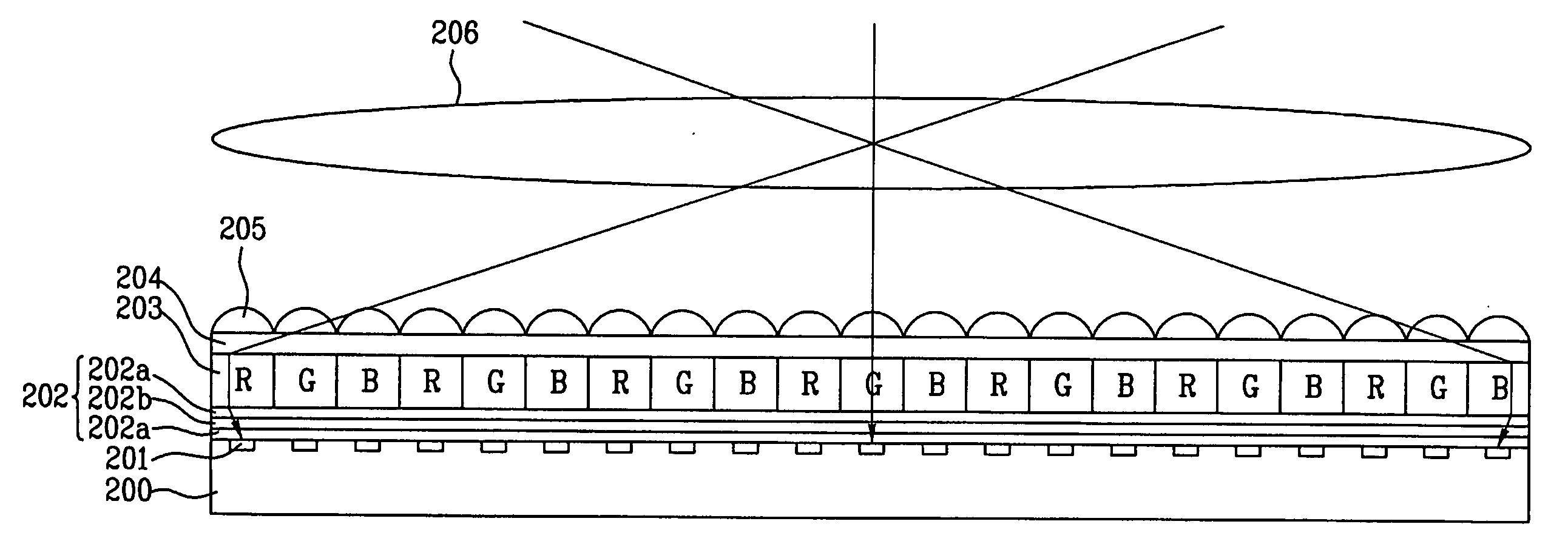
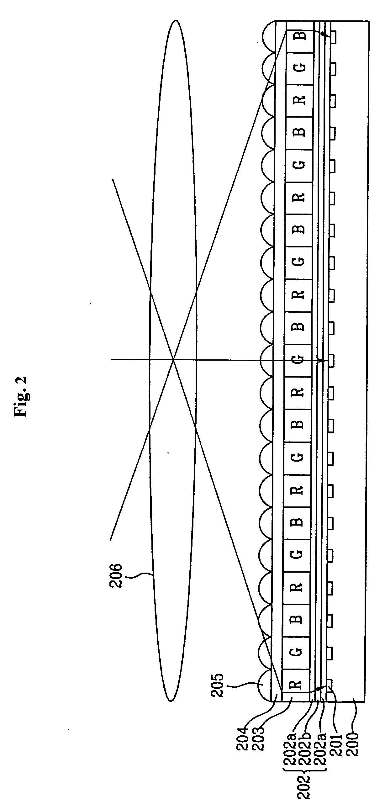
[0027]FIG. 2 is a sectional view of an image sensor according to an embodiment of the present invention.

[0028] Referring to FIG. 2, the image sensor according to an embodiment of the present invention includes a substrate 200 having a plurality of cell regions, photodiodes 201 formed in the cell regions of the substrate 200, an antireflection layer 202 that is formed above the substrate 200 including the photodiodes 201, a color filter layer 203 formed on the antireflection layer 202 to correspond to the photodiodes 201 of the cell regions, a planarization layer 204 formed on the color filter layer 203, and a plurality of microlenses 205 formed on the planarization layer 204 to correspond to the photodiod...


PUM


Abstract

An image sensor is provided. The image sensor includes a substrate having a plurality of cell regions, photodiodes formed in the cell regions of the substrate an antireflection layer, a color filter layer, a planarization layer, and a plurality of microlenses. The antireflection layer is formed above the substrate including the photodiodes and incorporates at least two insulating layers with different refractive indexes. The color filter layer is formed on the antireflection layer and corresponds to the photodiodes of the cell regions. The planarization layer is formed on the color filter layer. The plurality of microlenses is formed on the planarization layer and correspond to the photodiodes of the cell regions.

Description

RELATED APPLICATION [0001] This application claims the benefit under 35 U.S.C. §119(e) of Korean Patent Application Number 10-2005-0076151 filed Aug. 19, 2005, which is incorporated herein by reference in its entirety. FIELD OF THE INVENTION [0002] The present invention relates to an image sensor, and more particularly, to an image sensor and a method of fabricating the same, capable of minimizing a light loss caused by an incident angle of light. BACKGROUND OF THE INVENTION [0003] Generally, an image sensor is a semiconductor device that converts an optical image into an electrical signal. In a charge coupled device (CCD), metal-oxide-semiconductor (MOS) capacitors are very closely located to one another and charge carriers are stored in the capacitors and transmitted from the capacitors. In a complementary MOS (CMOS) image sensor, a switching method is employed using CMOS technology by forming MOS transistors in numbers as many as the number of pixels, and using a control circuit ...

Claims


Application Information

Patent Timeline
Patent Type & Authority Applications(United States)
IPC IPC(8): H01L27/148
CPCH01L27/1462H01L27/14645H01L27/14627H01L27/14621H01L27/146
Inventor SIK, KIM SANG
Owner DONGBU ELECTRONICS CO LTD
Why Eureka
Try Eureka