Dual work function buried gate type transistor and method for fabricating the same

a gate type transistor and dual work technology, applied in the field of transistors, can solve the problems of high work function, increased gate resistance, and difficult to reduce gate-induced drain leakage (gidl) in buried gate type transistors, and achieve the effect of reducing gate-induced drain leakage and improving current drivability

Active Publication Date: 2015-07-30
SK HYNIX INC
View PDF17 Cites 40 Cited by
  • Summary
  • Abstract
  • Description
  • Claims
  • Application Information

AI Technical Summary

Benefits of technology

[0010]Various embodiments of the present invention are directed to a buried gate type transistor and a

Problems solved by technology

However, a problem may be caused by the high work function since gate-induced drain leakage (GIDL) increases where the metal gate electrode and impurity regions overlap, that is, the source/drain regions.
Particularly, since the overlap area between a buried metal gate electrode and source/drain re

Method used


Image

  • Dual work function buried gate type transistor and method for fabricating the same
  • Dual work function buried gate type transistor and method for fabricating the same
  • Dual work function buried gate type transistor and method for fabricating the same

Examples


first embodiment

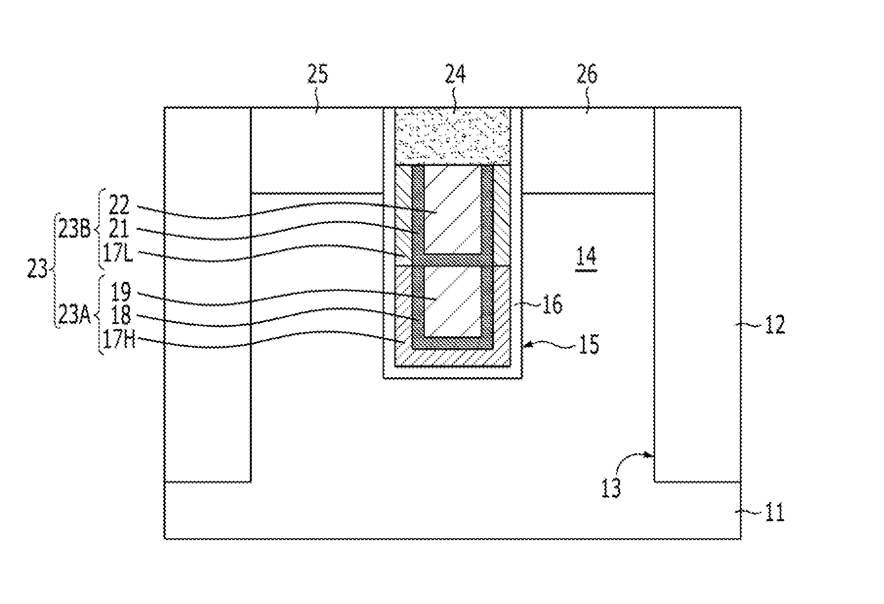
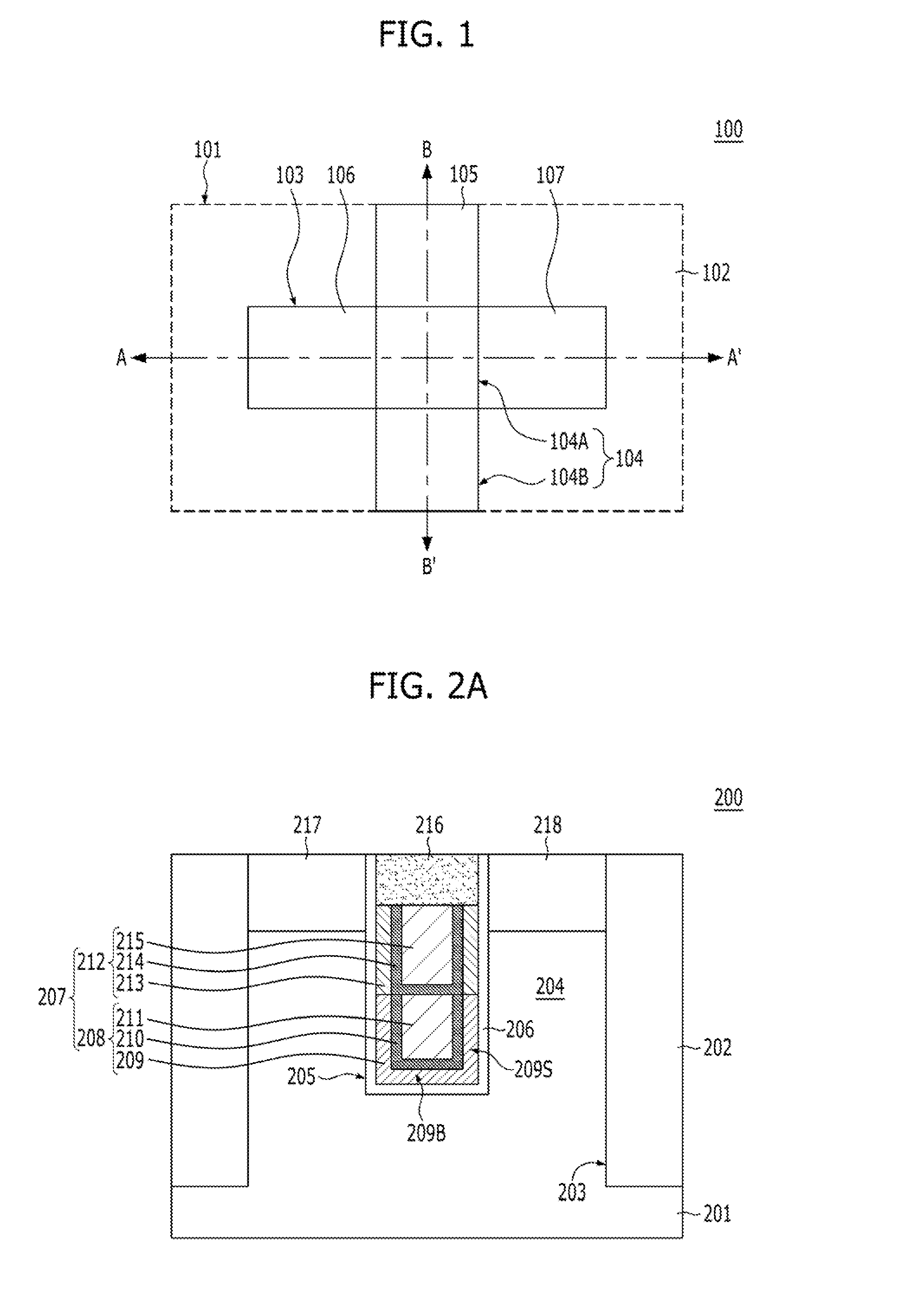
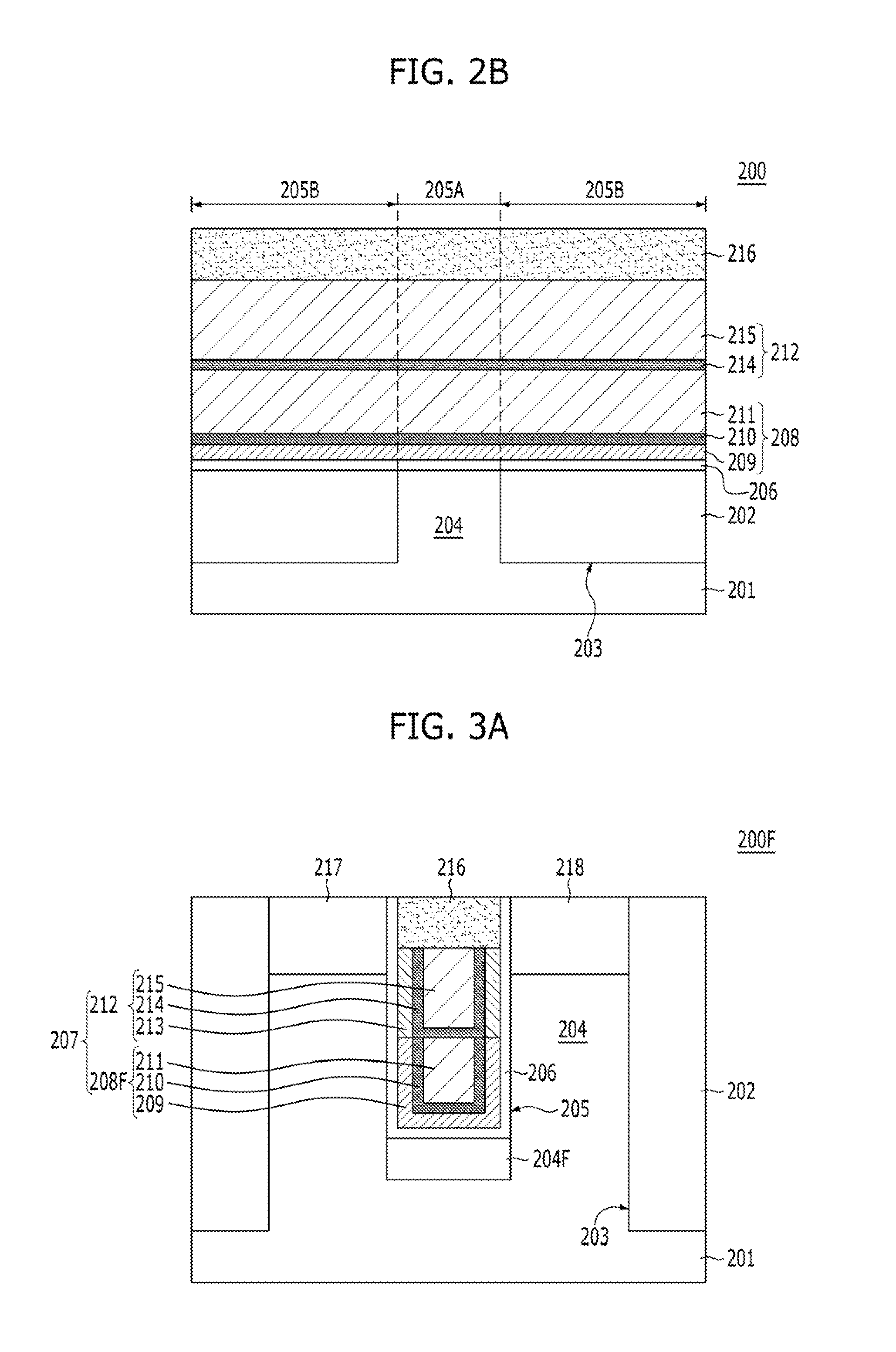
[0036]FIGS. 2A and 2B are views illustrating a transistor in accordance with the present invention. FIG. 2A is a cross-sectional view taken along the line A-A′ of FIG. 1. FIG. 2B is a cross-sectional view taken along the line B-B′ of FIG. 1.

[0037]A transistor 200 is formed in a substrate 201. The substrate 201 may include a semiconductor substrate. The substrate 201 may be a silicon substrate. An isolation layer 202 is formed in the substrate 201. The isolation layer 202 is filled in an isolation trench 203. An active region 204 is defined in the substrate 201 by the isolation layer 202.

[0038]A trench 205 which has a predetermined depth is defined in the substrate 201. The trench 205 may be a line type which extends in any one direction. The trench 205 has a shape which extends across the active region 204 and the isolation layer 202. The trench 205 has a depth that is shallower than the isolation trench 203. The trench 205 includes a first trench 205A and a second trench 205B, show...

third embodiment

[0083]FIGS. 6A and 6B are views illustrating a transistor in accordance with the present invention. FIG. 6A is a cross-sectional view taken along the line A-A′ of FIG. 1. FIG. 66 is a cross-sectional view taken along the line B-B′ of FIG. 1.

[0084]Referring to FIGS. 6A and 66, a transistor 300 is formed in a substrate 301. An isolation layer 302 is formed in the substrate 301. An active region 304 is defined in the substrate 301 by the isolation layer 302. The isolation layer 302 is filled in an isolation trench 303.

[0085]A trench 305 with a predetermined depth is defined in the substrate 301. The trench 305 may be a line type which extends in any one direction. The trench 305 has a shape which extends across the active region 304 and the Isolation layer 302. The trench 305 has a depth that is shallower than the isolation trench 303. The trench 305 includes a first trench 305A and a second trench 305B. The first trench 305A is defined in the active region 304. The second trench 305B ...

fourth embodiment

[0117]In a method for fabricating the transistor in accordance with the present invention, the remaining processes (not including the process for forming a fin region) are the same as shown in FIGS. 8A to 8F. For the process of forming a fin region, reference may be made to FIGS. 5A to 5D.

[0118]FIG. 9 is a view illustrating an exemplary semiconductor device including a transistor in accordance with the embodiments of the present invention.

[0119]Referring to FIG. 9, a semiconductor device 400 includes a first transistor 420 and a second transistor 440. The first transistor 420 and the second transistor 440 are formed in a substrate 401, and are isolated from each other by an isolation layer 402.

[0120]The first transistor 420 includes a buried gate electrode 406, a first source region 416, and a first drain region 417. The buried gate electrode 406 is formed in a trench 403. The trench 403 has a shape which extends across the isolation layer 402 and an active region 404. A first gate ...


PUM


Abstract

A transistor may include a source region and a drain region separately formed in a substrate, a trench defined in the substrate between the source region and the drain region, and a buried gate electrode formed. The buried gate electrode includes a high work function liner layer having a bottom portion which is positioned over a bottom of the trench and sidewall portions which are positioned on lower sidewalls of the trench; a low work function liner layer positioned on upper sidewalls of the trench, and overlapping with the source region and the drain region; and a low resistance layer contacting the high work function liner layer and the low work function liner layer, and partially filling the trench.

Description

CROSS-REFERENCE TO RELATED APPLICATIONS[0001]The present application claims priority of Korean Patent Application No. 10-2014-0011574, filed on Jan. 29, 2014, which is incorporated herein by reference in its entirety.BACKGROUND[0002]1. Field[0003]Exemplary embodiments of the present invention relate to a transistor, and more particularly, to a dual work function buried gate type transistor and a method for fabricating the same.[0004]2. Description of the Related Art[0005]A metal gate electrode is applied to a transistor. Gate resistance may be decreased by a metal gate electrode having a low resistance. Additionally, since the metal gate electrode has a high work function, channel dose may be decreased, leakage current may be reduced, and the performance of the transistor may be improved.[0006]However, a problem may be caused by the high work function since gate-induced drain leakage (GIDL) increases where the metal gate electrode and impurity regions overlap, that is, the source / dr...

Claims


Application Information

Patent Timeline
IPC IPC(8): H01L29/78H01L29/66H01L29/40H01L29/423
CPCH01L29/7827H01L29/4236H01L29/401H01L29/66484H01L29/66666H01L29/785H01L29/7813
Inventor OH, TAE-KYUNG
Owner SK HYNIX INC
Why Eureka
Try Eureka